Intel's Atom Architecture: The Journey Begins
by Anand Lal Shimpi on April 2, 2008 12:05 AM EST- Posted in
- CPUs
Poulsbo: An Unusually Revolutionary Chipset
In 2005 work began on the Poulsbo chipset, the ying to the Atom processor's yang. Much like the Atom processor itself, Poulsbo's design goal was simple: the focus was power and how to reduce it, even if it meant a performance hit.
The lead designers on Poulsbo had all worked on Intel's i840 chipset, one of the only desirable RDRAM chipsets of its time.
When Poulsbo was designed all of the available ICH designs were 130nm, and thus Poulsbo became 130nm as well. If you look at the pictures of the Atom processor and its chipset, it now makes sense why the chipset is so very huge.

The Intel Atom processor (left) vs. The Poulsbo chipset (right)
With Poulsbo being a 130nm part, it also helps explain why Atom is reserved for larger-than-iPhone devices today: the pair of chips simply wouldn't fit in anything too small. There are obvious power consumption concerns as well, but physically getting these two into a smartphone-sized device is going to be impossible until the next iteration.
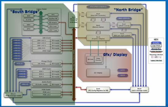
At a high level, Poulsbo looks to be no different than your run of the mill Intel chipset with integrated graphics:

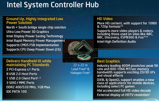
You'll quickly notice that the single chip solution, what Intel is calling a System Controller Hub (SCH) is a bit more unique. Instead of re-using a desktop chipset, Intel architected Poulsbo from scratch. In order to conserve power things like SATA and some of the USB ports were ripped out of the design. The designers chose to move back to PATA mostly because of power and smaller drives. Apparently in an idle state there isn't a power difference between PATA and SATA, but when actively transferring data SATA consumes much higher power due to its serial nature.
The FSB and memory frequencies are locked together which reduces power and PLL count. The chipset features a single channel DDR2-400/533 memory controller.
Poulsbo supports HD audio (Azalia, not the HD audio codecs) but reduced the number of audio engines supported in order to keep power under control. Only 2 channel audio is supported but you can access the audio interface externally, so conceivably you could dock an Atom device (such as a MID) and using an external codec get full 7.1 support.

The parts of Poulsbo
Intel also developed a fairly sophisticated message fabric to send data across the SCH - think of it as an on-chip Ethernet network for carrying things like interrupts and power management signals across the chip in an efficient manner.
Poulsbo introduces a new FSB to memory bridge that's much simpler than conventional designs. In most chipsets you have many different queues for traffic between the FSB and memory subsystem designed to extract the best possible performance from the platform. With Poulsbo the designers simply outfitted the memory controller with a large 8K memory and all FSB/memory traffic must go through that. The single memory storage made validation a lot easier, the chipset itself a lot smaller but could incur a performance hit. The MCH/North Bridge part of the SCH is around 20% of the area of what traditional MCH/North Bridges are thanks to this approach.
The ICH/South Bridge parts of Poulsbo are similarly trimmed. Years of legacy have been stripped out of the chipset, there's no parallel port, no floppy disk controller. In mainstream chipsets as long as someone is using the feature, it must be kept in play - the same wasn't true for Poulsbo. If the target market didn't need it, the feature wasn't going in the chipset.
The benefit of cutting the fat in Poulsbo is that the chipset was physically smaller with fewer gates, meaning lower leakage power.
In a highly atypical move for Intel, Poulsbo also supports non-standard 1.5V DDR2 memory. There's no official JEDEC spec for 1.5V DDR2 memory but many vendors have good enough modules that will work at 1.5V, so if an OEM wants to undervolt its memory the chipset will support it.
Much of the Poulsbo's design couldn't have been done had it not been for the Atom project. There are many revolutionary techniques at work within Poulsbo, it's a more modular design, a more efficient design and potentially holds the key to better chipset design in general - but none of these techniques were ever allowed to surface before.
Intel's chipset business is like a clock, every year a new platform is expected and some of the more revolutionary changes that could potentially interrupt the normal flow of things are generally frowned upon. Poulsbo, at least internally, broke down a lot of these barriers. While it's far from the highest performance chipset Intel has ever produced, Poulsbo requires roughly half the power of mainstream chipsets. Intel has been on an efficiency kick with its CPUs for a few years now, Poulsbo may help ignite a similar trend with chipsets as well.


46 Comments
View All Comments
lopri - Thursday, April 3, 2008 - link
This article is as much propagana-ish as it is technical. Did you read the last page of the article?clnee55 - Friday, April 4, 2008 - link
Since Anand wrote this article. I let him answer your accusationGulWestfale - Wednesday, April 2, 2008 - link
i believe that the graphics core in the chipset is a powerVR gen5 derivative; intel already uses some of their tech in its existing mainboards and wikipedia states that intel has licensed gen5 tech for one of its chipsets, the GMA500 (which is the same as poulsbo?) gen5 is also DX10-capable, which matches the info in your article.http://en.wikipedia.org/wiki/PowerVR#Series_5_.28S...">http://en.wikipedia.org/wiki/PowerVR#Series_5_.28S...
yyrkoon - Wednesday, April 2, 2008 - link
and wikipedia has been known to be wrong . . . a lot lately it seems.My point here *is*, I would probably trust anandtech more than wikipedia now days, as it seems any Joe can put up a 'reference' without citation.
jones377 - Wednesday, April 2, 2008 - link
Following the references link from the Wiki article...http://www.imgtec.com/News/Release/index.asp?NewsI...">http://www.imgtec.com/News/Release/index.asp?NewsI...
Poulsbo uses a PowerVR 3D core
Anand Lal Shimpi - Wednesday, April 2, 2008 - link
Yep, you guys are correct, I wasn't aware that it was public yet :) I've updated the article.Take care,
Anand