P55 Extreme Overclockers: Check your sockets!
by Rajinder Gill on October 15, 2009 12:01 AM EST- Posted in
- Motherboards
We start with a picture.
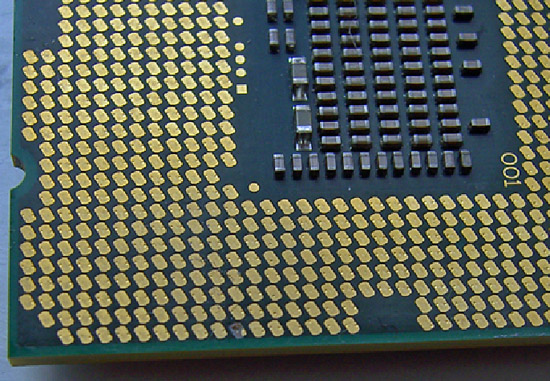
The picture above is after our Core i7 870 (LGA-1156) processor was overclocked up to 5.19GHz using our cascade with a -102° Celsius evaporator head temperature under full-load. Processor VCC power draw at these frequencies is around 160W (this is possible only due to subzero cooling), as measured with a clamp meter installed at the 12V EPS power lead. Study the pictures closely and you should notice something peculiar. Keep in mind it comes from a CPU installed in the same type of socket from a particular manufacturer.
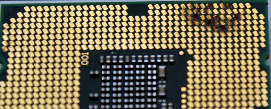
What happens after several extreme benchmark runs...
If you noticed something weird in the pictures then you understand the title of our article. We have what seems to be a potentially serious issue with proper socket loading on several P55-based motherboards when overclocking to the limit. We are of course not the only ones experiencing the problem as several of our overclocking peers have run into the same problem.
Normally we do not worry too much about mishaps during extreme overclocking testing as they are typically caused by factors outside of the supplier’s control. The overriding concern is that we have damaged every motherboard in our possession for the P55 overclocking (extreme) shootout as well as two very expensive i7/870 processors. These problems are the cause of a single component and are repeatable. As such, we thought we would provide details on current problems and will provide an update once all of the motherboard manufacturers affected have had a chance to properly respond.
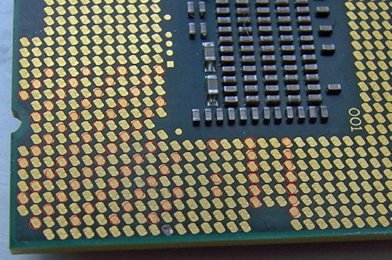
We draw your attention to the fact that the processor shown in this pictures exhibits signs of insufficient pin-to-pad contact (little to no contact) in what is a rather reproducible pattern with Foxconn manufactured 1156 sockets. As soon as an end-user mounts a CPU in a socket and latches the clamp mechanism, each pin should leave a notable mark on the associated pad.
We've marked locations where this does not seem to have happened, showing what appears to be a significant reduction in the number of VCC/VSS pins for proper power delivery, and certainly not at the right load line resistance. Damage resulting from highly overclocked use in these types of situations is not solely limited to the processor; let’s take a look at what happened to some of the motherboards in which these CPU were seated.
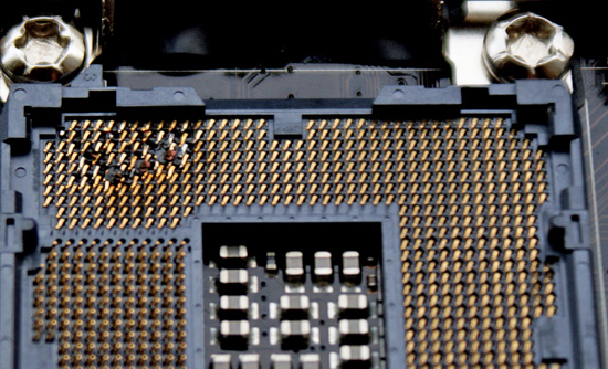
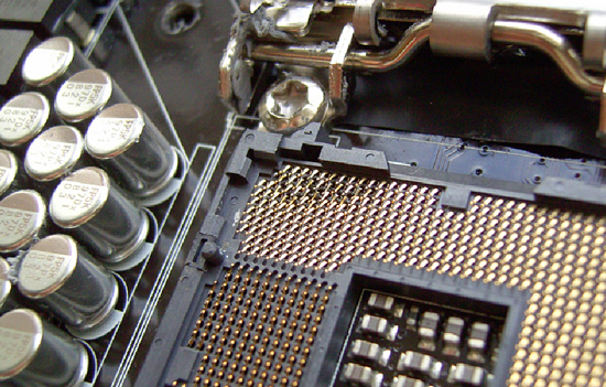
When Intel publishes socket specifications and design tolerances, it's up to component manufacturers to strictly adhere to them when designing, manufacturing, testing and ultimately selling their "compliant" components. Of course, that's not to say Intel could not have goofed when releasing their specification, leaving out a crucial tolerance or such. It could happen, but not likely. For the time being, let's assume that's not the case; seeing as how processors installed in sockets built by other companies have exhibited no such issue in testing to date.
At first glance, one might be inclined to think LGA-1156 based processors are intolerant of high-end overclocking, almost as if by design. This is correct to some extent; a quick glance at Intel’s white papers for socket 1156 CPU’s reveals that there are around 175 pads for VCC compared to over 250 for socket 1366 CPU’s. This means socket 1156 has around 66% of the current capacity of socket 1366, the caveat being that when overclocked, processors from both platforms draw similar levels of current.
When overclocked above 4GHz, processors from both platforms will draw around 15-16 amps via the EPS 12V rail to VCC, VTT and some of the other sub –system power rails under full 8 thread load from the Intel burn test (Linx). Assuming 85% PWM efficiency, we’re looking at power draw in the region of 130-140w to VCC on both platforms. The facts point toward tighter current handling tolerances for socket 1156 when compared to socket 1366, especially when it comes to non-connection of VCC/VSS power delivery pins.
Fortunately, we think we've been able to isolate pin to pad contact issues to one particular brand of parts. Physical inspection and end-user reports all but confirm the issues only affects sockets manufactured by Foxconn at this time. The only known alternative sockets in the wild are made by LOTES or Tyco AMP. We happen to have a couple of boards from EVGA using the LOTES/Tyco AMP sockets and MSI/DFI using the LOTES socket design, and thus far those boards have been issue free given highly similar operating conditions. In fact, we’ve managed to push our LGA-1156 processors further in heavy load tests on boards made using LOTES/Tyco AMP sockets than those made with sockets from Foxconn; something we’re not putting down solely to coincidence.
So far, EVGA is the only company we know that uses sockets exclusively from LOTES on their top-tier P55 boards - for example, the EVGA P55 Classified 200, model E659. This by the way may be the onus behind the decision to market the board’s “300% More Gold Content” socket statement as a purchasing option point. If you find yourself shopping for an EVGA P55 FTW, model E657, you've got a 50/50 chance of buying one with a Tyco AMP socket design (using a LOTES backplate), as opposed to one made solely with Foxconn's, the same goes for MSI and DFI who have batches of boards in the retail channel using LOTES sockets (although we're not entirely sure on socket specifics at this point). DFI told us earlier they have dropped usage of the Foxconn sockets completely until further notice. We hear the LOTES and Tyco AMP sockets are in short supply, which is probably why Foxconn's been able to fill the void in the market with what we believe to be a lower quality alternative for the extreme overclocker.
We took one of our damaged CPU’s and inserted it into one of the EVGA (LOTES/Tyco AMP) boards and took a few pics to show contact scoring and a side by side compare to the original Foxconn socket indents.
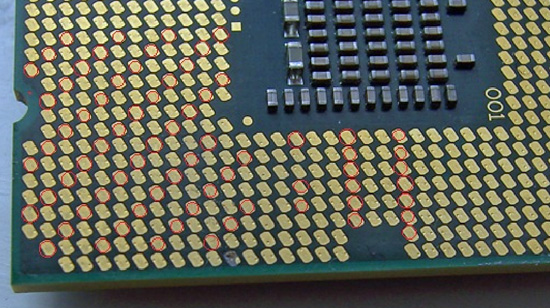
Foxconn 1156 Socket Installation
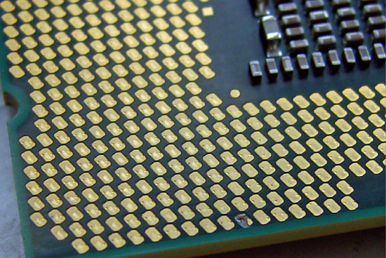
Tyco AMP / LOTES 1156 Socket Installation
Note how from a variety of angles certain pads show no evidence of contact from a Foxconn pin at all. Both the Tyco AMP and LOTES sockets have a larger pin/pad contact surface area leaving a slight scuff mark in the central area of each pad. In light of this, what we will say is that if you’re thinking of doing extreme overclocking on a board built using Foxconn's socket 1156, think again. Or, at least check your CPU for evidence of proper pin-to-pad contact.
We have not had any problems with air or water cooling overclocking up to 4.3GHz, although we do have a i5/750 that has developed a few dark pads after a thousand hours or so of constant overclocking. However, none of the boards have developed pin problems so we feel very safe in saying that any problems will probably occur only in extreme overclocking scenarios.
We also realize that partial responsibility for some of the less than acceptable CPU installations may be in fact due user installation errors. However, if users are screwing this up by doing nothing different than what they've always done when it comes to handling and installing LGA-type processors, then it's hard for us to find fault with the installer. Be aware of this situation and study the pin imprint on the CPU pads and make sure you have good contact on the VCC/VSS power delivery pads before pushing the system too hard.


273 Comments
View All Comments
neilmarzman - Friday, October 23, 2009 - link
Now that we are being civilized. Let me try to conjecture; based on my over 25 years of experience as a Professor of Electromagnetics, who still likes to tinker.If I had to make an educated guess, I will say that the ultimate responsibility lies with Intel. I am sure you will see this misalignment with Lotes sockets as well. It may not be visible to the naked eye, since if they are using more gold, the conductivity will improve, and as a result the Vtt pins will be able to withstand greater current draws, without leaving burn marks. However, it does not mean that all the data pins are making solid electrical contacts.
Power pins work with DC, so the impedance, (other than some indirect
EMI), is mostly resistance. Their inductance and capacitance do not play any role at all.
The inductance and capacitance which keep you guys from overclocking to the kingdom come, are the main impediments when designing a high frequency packaging. Since the silicon die itself, is not amenable to any fancy design work, since it is mostly on/off transistors. The nifty designing comes into play when packaging the silicon. The layout of the design at this point is critical, one misplaced pin will screw up the entire package (I meant the entire design). If there are sharp bends, if the traces are too close, if the traces are electrically too thin (compared to the wavelength); we will see huge instability. After the processor is packaged, it is necessary that this fine engineering is not frittered away by poor design starting from the pinout on.
Of course the first thing that processor sees on a board is the socket. If the mating mechanism is not foolproof, you lose all the advantage. I think it is the duty of the microprocessor manufacturer to make the processor packaging "idiot proof". Consider the case of these LGA sockets, the onus of this responsibility has been transferred to the socket manufacturers, who are small potatoes and who come an go. I did not see anything wrong with those zif sockets which required straight pins. They were almost foolproof: they had good contact and straight lines. The LGA socket has sharply bent conductor pins (for providing spring loading) which play hell with the impedance.
I am not sure that I understand the trade off. Unless Intel, somehow believes that as long as they can defend their microprocessors,they will be just fine; Even if the applications in which they are being used do not work. The customer usually does not care about these fine nuances. They quickly figure out that having "Intel Inside" is not a good thing ;-)
It is not about blame game, it is about providing a robust product to the consumer. Their ability to defend their processor will not protect them from tacking a hit.
Now, we all know that processors, have many parts, and as a result many features and full functionality is never tapped by everyday user application. With most people only using Office, email, chat, or watching porno, or playing games. Only when you run a mathematically intensive program you use can approach full tapping the processor capacity of a microprocessor. This is where these processors start to dump cores.
Keep in mind, that with all these new GPUs, most of graphical work is done outside the processor, so even graphically intensive applications will not put the processor through its paces. With P55 they are forcing the GPUs forcibly rely on the processor. This does is not to help out the consumer, this is mainly aimed at creating a bear-trap for their would be competitors:the GPU manufacturers, who now deserve a place at the table. There is no technical merit to it. In nature, when you dig holes for others; you can sometimes fall into them yourself, especially if you are not too bright. But I digress...
Moving along, usually the processor manufacturers can get away with serious follies. After all, how many people do any real computing?
Changing tracks, as promised, I installed an LGA166 processor into a Gigabyte EX58-UD5 yesterday. I did not experience any core dumps or any instability with normal chores. It too has a FOXcon socket; so I pulled out the processor and looked for pin impressions on the pads. Guess what? about 20% of the pins again did not make contact.
I think LGA1366 dodges the bullet, during normal use, because it does not have to work with a P55 and most of graphics does not need the help of the CPU.
In conclusion, my somewhat informed conjecture is that sockets LGA, are begging for a opportunity to fail. That is not what I would have expected from people at Intel; however mediocre their R&D people maybe. This is clear incompetence!
My very best,
Neil
dia - Friday, October 23, 2009 - link
Not sure I follow that ZIF sockets have no right angles in the transfer point from PCB to junction/clamp contact with the 'straight' CPU pins. Are you entirely sure about this? Or are we to assume that all Intel engineers know a lot less than you do about package design/layout/stray capacitance/inductance?So your 1156 CPU has around 230 non-connecting pads (you said around 20%)? Can you show pics to verify this, or does it only show up on your microscope? If some of those are signal pins and you're not experiencing 'odd behaviour', dropouts from the OS or even non-boots, one has to question if you're even looking for the right thing.
I'll be very surprised if there is no scuff mark showing contact on most of those pads. If you can't show pictures, I shall take a leaf out of your book and assume you have something to hide. I hope you're not referring to the pin prick indents from Intel's test jig socket. That would be funny and would certainly 'lower the ante'.
Rajinder Gill - Friday, October 23, 2009 - link
I've entered all the overclocked results I have on file to date into the graphing engine. These will go live sometime over the next few days hopefully (provided I get all the text finished and in for edit). A note of warning; the results are all sub-zero cooled, so won't interest to some of you. I will post up the actual screenshots too (just for those of you that doubt the benches were actually run..lol) These results were due to be posted with the socket issues in a single article but I had not finshed benching one of the LOTES based boards (just finshed that this week - EVGA E659).No further info yet from any vendors regarding sockets/non pin contact or otherwise. I'll stick up the results I have regardless.
later
Raja
Rajinder Gill - Friday, October 23, 2009 - link
BTW, here are some of the results I uploaded via imageshack. Just to prove the benches were actually run @ sub-zero ;)http://img62.imageshack.us/img62/6015/235firstrun....">http://img62.imageshack.us/img62/6015/235firstrun....
http://img185.imageshack.us/img185/6996/wprime5177...">http://img185.imageshack.us/img185/6996/wprime5177...
http://img93.imageshack.us/img93/5511/wprime5222e6...">http://img93.imageshack.us/img93/5511/wprime5222e6...
http://img5.imageshack.us/img5/8672/237crop.jpg">http://img5.imageshack.us/img5/8672/237crop.jpg
Plenty more on file, final results will be up in grpahs for easy cross compare and also highlighting where we lost a board.
ClagMaster - Friday, October 23, 2009 - link
Impressive overclock results -- even with Liquid N2. Did any of the sockets fail while these benchmarks were being run?Raja. I saw a posting at CPU3D which featured this article which quoted you by name.
http://www.techreport.com/discussions.x/17773">http://www.techreport.com/discussions.x/17773
There was a quote of an engineer working at Intel:
"Think about it ... at 1.65V, you are around 250watts ... this is 150AMPS!gigabyte gave what the Overclockers asked ... now, use it with moderation ... I tested on a mecanical [sic] thermal dummy ... the [Gigabyte GA-P55-UD6] can deliver up to 160AMPS without occilation [sic] ... at this point, you are more than 2x the specs for currents ... and 60% over the voltage ... and 263% of the based power ..."
"my guess in those cases is "finger print" or oxidation due to [liquid nitrogen] condensation plus an incredible UD6 voltage supply that does not bend under load. (thing requested by the OC community)"
I still think operating the i5/i7 at stock speeds for a Foxconn LGA 1156 will not result in failed sockets.
Rajinder Gill - Friday, October 23, 2009 - link
Hi,Yes I lost one of my boards during these benches.
That 'Intel' response is from Francois. He's got a point but I'm not sure if grubby marks on the pads are the cause given that most of the VCC related burnout happen on the same part of the land. I'm not sure we'll ever get a fully informed technical response as to the exact cause but you never know.
later
Raja
neilmarzman - Thursday, October 22, 2009 - link
Funny, so you were around for the QWERTY keyboard... interesting :-)Experimenting? With what?
If you cannot read critically, my only purpose is to remind this site that integrity counts for something. Instead of getting in bed with the manufacturers. They should try to report their findings without sugarcoating. I am sure you are not unaware of phenomenon of whoring for access.
Anand or anandtech is small potatoes for me to defame. It is the monitory harm he is causing to his readership which concerns me more.
However, I do not question his right to do whatever will get him the most money in the shortest time. That is his birthright. If in doing so he kills the goose which lays the golden egg; that is also his business.
I think that this site is opening itself up to potential litigation by cheer-leading for manufacturers by intentionally providing or withholding selective information/misinformation, just like CNBC used to do, and I would hate to see that.
If you have a background in electrical engineering, more power to you. I was merely mentioning "a finishing school" :-) It that a big enough ante for you?
None of you guys have the equipment to test anything including those at Anandtech. Running a few test suits, or measuring total input current is not real testing. Again it is more in line with souping up your car (a la Tim Allen and his lawn-mower). My gardener likes to indulge souping up his car, he has a 1000 horsepower engine, with N20 injection in it. The trouble is that it always broken: an axle here, a burned out clutch there. He even managed to explode his engine. To me that is overclocking, and that is fine with me. However, when I buy something I want to know if it will perform within manufacturer's specifications.
Doesn't it bother you that the data pins are not making contact, and the only reason they stumbled upon the partial reason was ironic serendipity... by looking at burn marks! That is as low tech as you can get. I am going to check out a socket LGA1366 as well and see if FOXCon is getting a bum rap (it is easy to finger the small guy). It could as easily be a design flaw on part of Intel. After all, both the socket or processor pads can miss the tolerances.
BTW, the amount of gold used has nothing to do with placement or strength of contacts, it only affects the conductivity if physical contact is made. On the other hand, the issue of placement affects the total impedance even if no contact is made, two out of the three elements of impedance still play their role. This was another ridiculous canard.
Regards,
Neil
Porksmuggler - Wednesday, October 21, 2009 - link
you're not exactly "upping the ante" with this rambling about Betamax and RISC, and yes many of us were around for both. You seem to post only to insult the author, Anand, overclockers, and Intel. If you have a different agenda, please let it be known.My background is in electrical engineering, I do not own a "souped up" car or any burnt out computers. I did get a laugh out of the imagery though :) Believe it or not, there are many overclockers who do it for the sake of experimentation alone. It's not about being penny-wise pound foolish, regardless of the stereotype you have created in your mind. As I mentioned before, if you do not have the knowledge, or the resources, perhaps you should abstain.
JDD - Tuesday, October 20, 2009 - link
I just don’t understand all of this jibber jabber dimples or not if you install the chip and every pad is not making contact with a corresponding point on the socket. It’s not right. Fix it. End of story. This is not about how much you can get away with. Overclocking or not. Fix it. That’s it. There should be no more discussion. Than just Fix itdingetje - Tuesday, October 20, 2009 - link
so does yours have dimples or not? ;)