Radeon 5970 Overclocking: The VRM Temperature Bottleneck
by Ryan Smith on November 25, 2009 12:00 AM EST- Posted in
- Ryan's Ramblings
In our Radeon HD 5970 review, we ran in to some issues when trying to overclock the card to 5870 speeds of 850MHz/1200MHz. At the time this is something we attributed to the VRMs, meanwhile AMD suggested that it was cooling related, and that we should manually increase the fan speed.
As it turns out, we were both right, we just didn’t have the tools at the time to properly identify and isolate the issue. Late last week we got our hands on a beta version of Everest Ultimate, which added preliminary support for the 5970. With that, we could read and log the voltages and temperatures of the various components of the 5970, and properly isolate the issue.
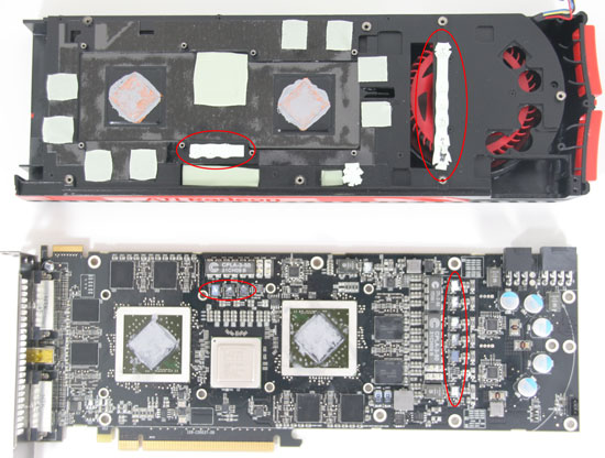
From that, we’ve discovered a few interesting things about the 5970. Let’s start things off with the cooler removed from the 5970.
We’ve gone ahead and circled the VRMs in red. There are 9 altogether; 6 on the right side, and 3 near the left side of the card. We aren’t able to track down what each specific VRM is connected to, but we believe that each GPU is attached to 3, each GPU’s RAM is attached to 1, and finally the PLX PCIe bridge is attached to 1. Regardless, pay attention to the location of these VRMs for later discussion.
As we previously noted in our 5970 review, when overclocked the card was throttling down in two cases. One was when running OCCT/FurMark, members of AMD’s “power virus” list by virtue of the fact that they put a card under a greater load than AMD believes to be realistically possible. Our 5800 series cards never throttled under these applications, so to see the 5970 throttle here was a bit surprising but not wholly unexpected.

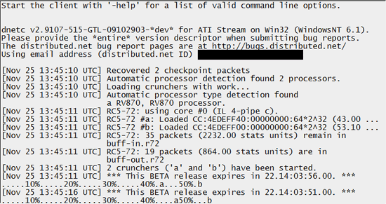
The second case was using Distributed.net’s pre-release GPU client for use with AMD’s GPUs. Since this is a real program, this was absolutely unexpected, and is what instigated our look in to the matter.
In both cases, the key was the overall load on the GPU cores, and consequently the amount of power required to drive the GPUs. When a bank of VRMs reached roughly 120C (this being averaged among all the VRMs in that bank), overcurrent protection kicked in and throttling began. In the case of FurMark this was very quick and even at 100% fan speed the cooler could still not keep the VRMs cool enough to allow full-time 850MHz operation. The Dnet client on the other hand was much slower to ramp up, and we ultimately found that 70% fan speed was enough to keep our hottest bank of VRMs below the threshold, stabilizing at 116C.
Notably, during this whole period the GPU cores themselves stayed at or under 94C, which is still a few degrees below their own throttle point. AMD’s fan quickly ramped up, and in our testing it only needed to go to 59%. So if the cores did get hotter there was still plenty of room to go with the fan.
This brings us to our first point of concern for the 5970, which is the fan speed. Clearly it’s adequate for the GPU cores themselves, but we cannot find any proof that the fan speed is adjusted based on the temperature of the RAM or the VRMs. If the fan speed were to ramp up in the case of near-critical temperatures in the VRMs, then the Dnet client likely would have ran without an issue the first time, as this would have pushed the fan to 70%.
We asked AMD about whether the fan speed is affected by VRM temperatures at all, but we didn’t receive a response. This isn’t particularly surprising since post-launch periods are a good time to take a vacation and there’s a holiday this week for their American employees, but it means we couldn’t get a confirmation of our assumption. So for the time being, we’re working on the assumption that only GPU core temperatures drive fan speed.
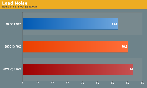
It also bears mentioning that the 5970 gets quite a bit louder when the fan goes up to 70%. We went ahead and captured the noise data for it at 70% and 100%, which is in the chart below. At the 70% fan speeds needed to run the Dnet client at 5870 speeds, you’re looking at 70dB, which is quite a bit louder than the fan noise at stock speeds. It is in fact uncomfortably loud by this point.

Our second point of concern goes beyond just the fan, and is the overall cooling of the VRMs. When we looked at our Everest logs after running the Dnet client, we noticed something interesting with respect to which VRMs were overheating. The VRM bank attached to GPU 1 was some 25C hotter under load, but it wasn’t GPU 1 that was the hottest. GPU 2 was consistently a couple of C warmer. We don’t believe this to be in error, so to understand why this is, we refer back to our disassembled 5970.
As the fan is on the right, the right side of the heatsink the vapor chamber dumps its heat in to is going to be cooler than the left side by the virtue of the fact that the left side is effectively using the already hot-air of the right side to cool. The heatsink and vapor chamber mitigate this some, but the right side of the card – and consequently the right GPU– should be cooler than the left side. This leads us to believe that GPU 1 is the right GPU, and GPU 2 is the left GPU.
This is important since if we look at the VRMs, the VRMs feeding GPU 2 sit under the vapor chamber, while the VRMs feeding GPU 1 (along with the RAM and PCIe bridge) are not. We haven’t been able to fully dissect the cooler, but the VRMs on the right side sit right underneath the fan, and we don’t believe there to be a significant heatsink in the metal bar that sits above them. So while the VRMs feeding GPU 2 are being cooled by the vapor chamber, the VRMs feeding GPU 1 are only being cooled by the heat dissipation properties of a metal bar.
From this, we can conclude that the VRM banks are receiving wildly different amounts of cooling. The VRMs on the right side are not cooled nearly as well as those on the left and as a result the card is being held back by the VRMs on that right side. To that extent, we believe that if all the VRMs received the same level of cooling as the VRMs on the left side, then the card would have no problem maintaining 5870 speeds while running the Dnet client, and likely even FurMark. It’s also worth noting that all the 5800 series cards share the design of placing the VRMs under a metal bar under the fan, but the 5970 seems to suffer more for it compared to the 5800 series.
Finally, there’s the matter of whether this is even going to matter for most users. After catching the VRMs hitting 120C under the Dnet client, we went looking at other applications and games to see where else the card was throttling. The result of that inquiry was that we couldn’t find anything else that could match the Dnet client in total load. The Dnet client is a bit of a special case here, since crunching encryption keys makes exceedingly good use of the 5-wide SIMD design in the 2000-5000 series cards. When we took a look at something similar to the Dnet client, in this case the Folding@Home GPU client, we couldn’t break 100C. The significance of that result remains to be seen though, since the Folding@Home GPU client hasn’t been optimized for the 5800/5900 series yet like the Dnet client has. Our ultimate concern is that this card is going to repeatedly fall flat on its face at 5870 speeds with more GPGPU applications as OpenCL and DirectCompute take off, and the number of such applications bloom.
| Radeon HD 5970 Temperatures | ||||
| GPU 1 Temp | GPU 1 VRM Temp | GPU 2 Temp | GPU 2 VRM Temp | |
| FurMark | 89C | 110C | 91C | 83C |
| Dnet Client | 87C | 101C | 88C | 77C |
| FurMark OC | 91C | 120C | 94C | 100C |
| Dnet Client OC | 93C | 120C | 94C | 94C |
| Cryis Warhead OC | 87C | 96C | 89C | 74C |
| STALKER OC | 85C | 96C | 88C | 72C |
Meanwhile in games it was a similar story. Crysis and the STALKER benchmark are two of the most demanding games we’ve tested on the 5970, and in both cases the VRMs again peaked at near 100C. As games aren’t going to hammer the SIMDs like GPGPU applications do, the power load from games should be lower than for GPGPU applications.
As far as our opinion on the 5970 is concerned though, this doesn’t change anything. While we’ll buy AMD’s “power virus” rationale for FurMark and OCCT, the Dnet client is not a power virus. It’s a real application, one that AMD even used in their 5800 presentation back in September. Thus as far as we’re concerned, our 5970 is only good for 775MHz, the lowest clock speed where the VRMs stayed under 120C. Granted, AMD will never officially promise that the 5970 can reach 5870 speeds, but based on how the 5970 was promoted and presented the fact of the matter is that the card can’t meet its advertised capabilities – this card is clearly meant for 5870 clockspeeds.
With that in mind, we’ll end on two thoughts. The first of which is that in spite of our experience, for pure gaming scenarios we don’t have any data to bring in to doubt the idea that the card can run at 5870 speeds without throttling. So long as you only intend to play games, those speeds should be fine.
Our second thought is that cards from vendors with custom overclocking utilities will be better able to maintain 5870 speeds at all times. These are cherry-picked chips, so there’s no reason why they absolutely need 1.1625v core voltage to run at 850MHz; we suspect that they could do with less. Since voltage is our main enemy here, even a small drop in voltage should have a noticeable impact on VRM temperatures. But you’re going to need a utility with a full suite of voltage options to take advantage of that.


45 Comments
View All Comments
Ryan Smith - Wednesday, November 25, 2009 - link
Your eyes deceive you. There are only 9 VRMs. I think I see what you mean, that's just another small chip.largon - Thursday, November 26, 2009 - link
Fact is, there are not just 9, and not even 10 but 13 pieces of VRMs of various models of Volterra slave chipsets and other non-Volterra parts on the card.Here's a complete list:
- 3× Volterra VT1157SFs silkscreened as "U71, U72 and U73" located above the PLX, coupled with the lone horizontal CPLA-3-50 choke "L22/L23". These feed the GPU silkscreened as "U1". Controlled by the VT1165MF marked as "U70".
- 3× Volterra VT1157SFs silkscreened as "U87, U88 and U89" coupled with the vertical CPLA-3-50 choke "L26/L27". located to the right of GPU on the right. These feed the GPU silkscreened as "U2". Controlled by the VT1165MF marked as "U86".
- 2× Volterra VT1157SFs silkscreened as "U76 and U77" coupled with the vertical CPLA-2-50 choke "L21". These feed RV870 GPU "uncore" I/O (GDDR5 ctrl?), 2 phases shared for both GPUs. Controlled by the VT1165MF marked as "U75".
- 1× Volterra VT232WF silkscreened as "U60" coupled with a 1005R1 choke "L14", located above GPU "U2". This feeds the GDDR5 chips their VDD or VDDQ (no way to tell which just by looking).
- 1× Volterra VT232WF silkscreened as "U60" coupled with a 1005R1 choke "L15", located below the vertical CPLA-3-50. This feeds the GDDR5 chips their VDD or VDDQ (no way to tell which just by looking).
- 2× Infineon n-channel MOSFETs (042N03LS + 119N03S) silkscreened as "Q1" and "Q2", respectively, coupled with a 1R5 choke "L1" located on the bottom edge of the PCB, below and left of the vertical CPLA-3-50. These are for the PLX bridge chip.
- 1× AOSMD (AO)Z1024DI low-power integrated buck regulator coupled with a 4R7 choke "L33" located above the vertical CPLA-2-50 choke "L21". I don't know what purpose it serves.
mindless1 - Thursday, November 26, 2009 - link
Thank you!largon - Thursday, November 26, 2009 - link
Correcting a few typing errors:- 1× Volterra VT232WF silkscreened as "U61" coupled with a 1005R1 choke "L15", located below the vertical CPLA-3-50. This feeds the GDDR5 chips their VDD or VDDQ (no way to tell which just by looking).
- 2× Infineon n-channel MOSFETs (042N03LS + 119N03S) silkscreened as "Q2" and "Q1", respectively, coupled with a 1R5 choke "L1" located on the bottom edge of the PCB, below and left of the vertical CPLA-3-50. These are for the PLX bridge chip.
Mr Perfect - Wednesday, November 25, 2009 - link
It looks like one of the VRMs on the right didn't even touch the heatsink, it has no thermal goop on it and there is n oindentation on the TIM either. Maybe better contact would help? Is Anand's card similar or wose for contact? Could be a quality control thing.greywood - Wednesday, November 25, 2009 - link
Second that - - from the photo, it looks like at least two VRM's at the bottom right side and all three at the top center are making little if any contact with the TIM. Might be interesting to clean off the generic goop, re-apply some AS5 (or such) then really "cinch-down" the HSF and try re-testing?Rajinder Gill - Wednesday, November 25, 2009 - link
I think Ryan scraped that off to read off the FET part numbers. I asked him the FET model numbers because I wanted to find out if ATI had used 45amp slaves.Ryan Smith - Wednesday, November 25, 2009 - link
Bingo. The clean VRM is the one I scraped clean to get the model number.Rajinder Gill - Thursday, November 26, 2009 - link
Each VGPU FET is spec'd at 40 amps. So 120 amps tops per GPU.regards
Raja
mindless1 - Thursday, November 26, 2009 - link
Spec'd at 40 amps if they had adequate copper under them, ++ heatsinking on top