Original Link: https://www.anandtech.com/show/13282/nvidia-turing-architecture-deep-dive
The NVIDIA Turing GPU Architecture Deep Dive: Prelude to GeForce RTX
by Nate Oh on September 14, 2018 12:30 PM EST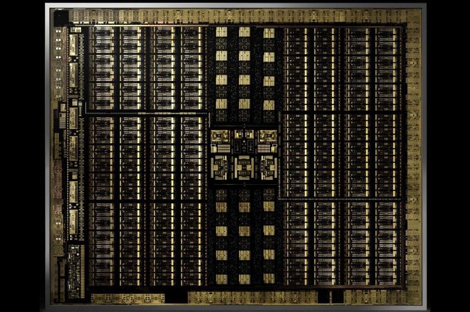
It’s been roughly a month since NVIDIA's Turing architecture was revealed, and if the GeForce RTX 20-series announcement a few weeks ago has clued us in on anything, is that real time raytracing was important enough for NVIDIA to drop “GeForce GTX” for “GeForce RTX” and completely change the tenor of how they talk about gaming video cards. Since then, it’s become clear that Turing and the GeForce RTX 20-series have a lot of moving parts: RT Cores, real time raytracing, Tensor Cores, AI features (i.e. DLSS), raytracing APIs. All of it coming together for a future direction of both game development and GeForce cards.
In a significant departure from past launches, NVIDIA has broken up the embargos around the unveiling of their latest cards into two parts: architecture and performance. For the first part, today NVIDIA has finally lifted the veil on much of the Turing architecture details, and there are many. So many that there are some interesting aspects that have yet to be explained, and some that we’ll need to dig into alongside objective data. But it also gives us an opportunity to pick apart the namesake of GeForce RTX: raytracing.
While we can't discuss real-world performance until next week, for real time ray tracing it is almost a moot point. In short, there's no software to use with it right now. Accessing Turing's ray tracing features requires using the DirectX Raytracing (DXR) API, NVIDIA's OptiX engine, or the unreleased Vulkan ray tracing extensions. For use in video games, it essentially narrows down to just DXR, which has yet to be released to end-users.
The timing, however, is better than it seems. A year or so later could mean facing products that are competitive in traditional rasterization. And given NVIDIA's traditionally strong ecosystem with developers and middleware (e.g. GameWorks), they would want to leverage high-profile games for ringing up consumer support for hybrid rendering, which is where both ray tracing and rasterization is used.
So as we've said before, with hybrid rendering, NVIDIA is gunning for nothing less than a complete paradigm shift in consumer graphics and gaming GPUs. And insofar as real time ray tracing is the 'holy grail' of computer graphics, NVIDIA has plenty of other potential motivations beyond graphical purism. Like all high-performance silicon design firms, NVIDIA is feeling the pressure of the slow death of Moore's Law, of which fixed function but versatile hardware provides a solution. And where NVIDIA compares the Turing 20-series to the Pascal 10-series, Turing has much more in common with Volta, being in the same generational compute family (sm_75 and sm_70), an interesting development as both NVIDIA and AMD have stated that GPU architecture will soon diverge into separate designs for gaming and compute. Not to mention that making a new standard out of hybrid rendering would hamper competitors from either catching up or joining the market.
But real time ray tracing being what it is, it was always a matter of time before it became feasible, either through NVIDIA or another company. DXR, for its part, doesn't specify the implementations for running its hardware accelerated layer. What adds to the complexity is the branding and marketing of the Turing-related GeForce RTX ecosystem, as well as the inclusion of Tensor Core accelerated features that are not inherently part of hybrid rendering, but is part of a GPU architecture that has now made its way to consumer GeForce.
For the time being though, the GeForce RTX cards are not released yet, and we can’t talk about any real-world data. Nevertheless, the context of hybrid rendering and real time ray tracing is central to Turing and to GeForce RTX, and it will remain so as DXR is eventually released and consumer-relevant testing methodology is established for it. In light of these factors, as well as Turing information we’ve yet to fully analyze, today we’ll focus on the Turing architecture and how it relates to real-time raytracing. And be sure to stay tuned for the performance review next week!
Ray Tracing 101: What It Is & Why NVIDIA Is Betting On It
Because one of the two cornerstone technologies of the Turing architecture is NVIDIA’s ray tracing RT cores, before we dive too much into the Turing architecture, it’s perhaps best to start with a discussion on just what ray tracing is. And equally important, why NVIDIA is betting so much silicon on it.
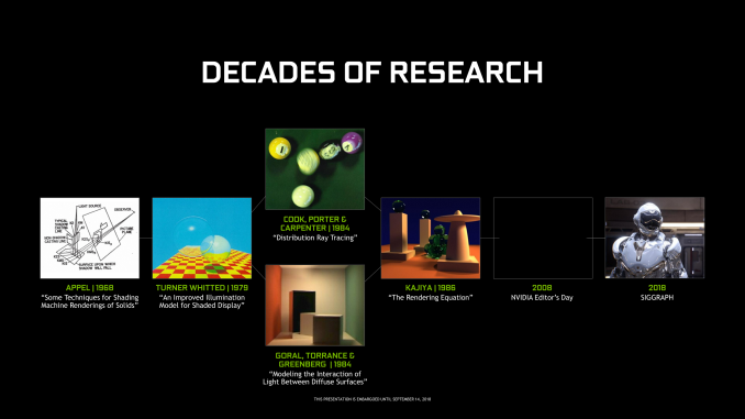
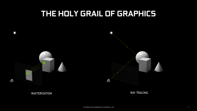
Ray tracing, in short, is a rendering process that emulates how light behaves in the real world. From a fundamental (but not quite quantum physics) level, light can be considered to behave like a ray. This is because photons, outside other influences, will travel in a straight line until they hit something. At which point various interactions (reflection, refraction, etc) occur between photons and the object.
The catch with ray tracing is that it’s expensive. Incredibly expensive. The scale of the problem means that if you take a naïve approach and try to calculate all of the rays of photons emitting from every light source in a scene, you’re going to be tracing an uncountable, near-infinite number of rays bouncing around a scene. It is essentially modeling all of the physical interactions of light within a bounded space, and that’s an incredible number of interactions.
As a result there have been a number of optimizations developed for ray tracing over the years. Perhaps the most important of which is sort of turning the naïve concept on its head, and instead of tracing rays starting from light sources, you instead go backwards. You trace rays starting from the point of the observer – essentially casting them out into a scene – so that you only end up calculating the light rays that actually reach the camera.
Such “reverse” ray tracing cuts down on the problem space significantly. It also means that conceptually, ray tracing can be thought of as a pixel-based method; the goal is to figure out what each pixel should be.
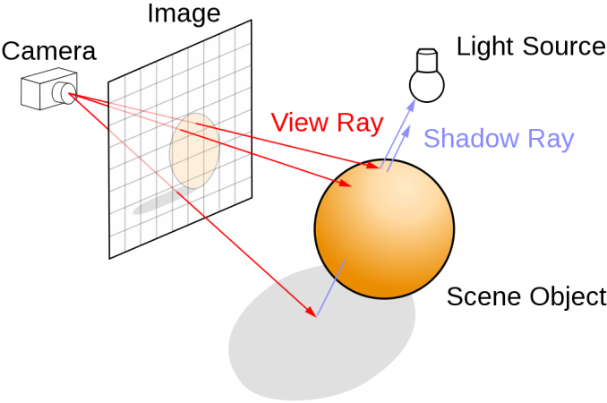
Ray Tracing Diagram (Henrik / CC BY-SA 4.0)
However even with this optimization and others, ray tracing is still very expensive. These techniques make ray tracing cheap enough that it can be done on a computer in a reasonable amount of time, where “reasonable” is measured in minutes or hours, depending on the scene and just how precise and clean you want the rendered frame to be. As a result, anything other than the cheapest, grainiest ray tracing has been beyond the reach of real-time rendering.
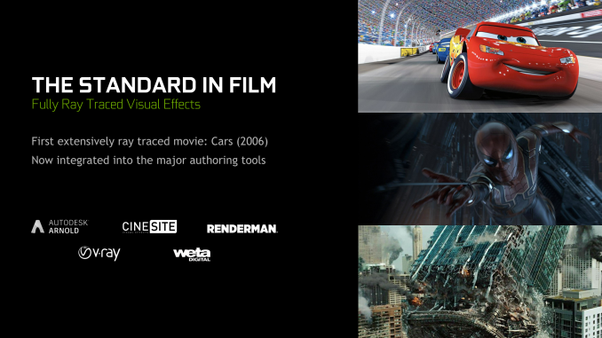
In practical terms then, up until now ray tracing has been reserved purely for “offline” scenarios, particularly 3D graphics in movies. The quality of ray tracing makes it second to none – it’s emulating how light actually works, after all – as it can accurately calculate reflections, shadows, light diffusion, and other effects to a degree of accuracy that no other method can. But doing all of this comes at a heavy cost.
Enter Rasterization: The World’s Greatest Hack
The high computational cost of ray tracing means that it hasn’t been viable for real-time graphics. Instead, since the earliest of days, the computing industry has turned to rasterization.
If ray tracing is a pixel-based approach, then rasterization would be called a polygon-centric approach to 3D rendering. But more than that, rasterization is a hack – a glorious hack to get around the fact that computers aren’t (or at least, weren’t) fast enough to do real-time ray tracing. Rasterization takes a number of shortcuts and makes a number of assumptions about how light, objects, and materials work in order to reduce the computational workload for rendering a scene down to something that can be done in real time.
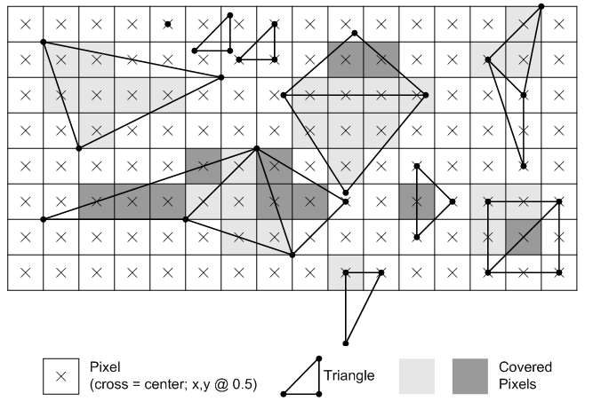
Rasterization at its most basic level is the process of taking the polygons in a scene and mapping them to a 2D plane, the pixel grid. This means polygons are sorted and tested to see which polygons are actually visible, and then in various stages, these polygons are textured, shaded, and otherwise processed to determine their final color. And admittedly this is a gross simplification of a process that was already a simplification – I’m completely ignoring all the math that goes into transforming 3D objects into a 2D representation – but in an amusing twist of fate, the hack that is rasterization is in some ways more complex than the natural process of ray tracing.
The key point to rasterization is not so much how it works, but rather that it doesn’t use rays, and therefore it’s cheap. Very cheap. And better still, it can be done in parallel. As a result GPUs have arisen as incredible matrix multiplication machines, and are capable of testing hundreds of millions of polygons every second and coloring billions of pixels. With a few exceptions, rasterization is nice and orderly, allowing computational techniques like Single Instruction Multiple Data/Thread (SIMD/SIMT) to do the necessary processing with incredible efficiency.
The catch to rasterization is that because it’s a hack – however glorious it is – at the end of the day there are limitations to how well it can fake how vision and light work in the real world. Past basic polygon projection and texturing, pixel shading is where most of the work is done these days to actually determine what color a pixel needs to be. It’s in pixel shaders that the various forms of lighting (shadows, reflection, refraction, etc) are emulated, where distortion effects are calculated, etc. And pixel shaders, while powerful in their own right, are not capable of emulating real light to a high degree, at least not in a performant manner.
It’s these limitations that lead to the well-publicized drawbacks in rasterization. The unnatural light, the limited reflections, the low resolution shadows, etc. Now conceptually, it is by no means impossible to resolve these issues with rasterization. However the computational cost of doing so is very high, as the nature of rasterization is such that it’s difficult to bolt on such high accuracy methods on to what’s at its core a hack. Rasterization is meant to be quick & dirty, not accurate.
Ray Tracing Returns – Hybridization
Coming full-circle then, we reach the obvious question: if rasterization is so inaccurate, how are games meant to further improve their image quality? Certainly it’s possible to continue going down the road of rasterization, and even if the problem gets harder, image quality will get better. But keeping in mind that rasterization is a hack, it’s good to periodically look at what that hack is trying to achieve and whether that hack is worth the trade-offs.
Or to put this another way: if you’re going to put in this much effort just to cheat, maybe it would be better to put that effort into accurately rendering a scene to begin with?
Now in 2018, the computing industry as a whole is starting to ask just that question. Ray tracing is still expensive, but then so are highly accurate rasterization methods. So at some point it may make more sense to just do ray tracing at certain points rather than to hack it. And it’s this train of thought that NVIDIA is pursuing with great gusto for Turing.
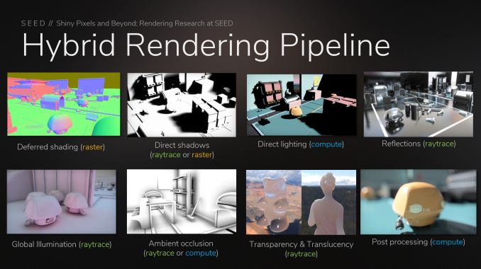
For NVIDIA, the path forward is no longer pure rasterization. Instead their world view is one of hybrid rendering: combining the best parts of rasterization and compute with the best parts of ray tracing. Just what those parts are and where they should be done is a question ultimately up to developers, but at a high level, the idea NVIDIA is putting forth is to use ray tracing where it makes sense – for lighting, shadows, and everything else involving the interaction of light – and then using traditional rasterization-based methods for everything else.
This means that rather than immediately jumping from rasterization to ray tracing and losing all of the performance benefits of the former, developers can enjoy the best of both worlds, choosing how they want to balance the performance of rasterization with the quality of ray tracing. The examples NVIDIA and its partners have pitched thus far have been the low-hanging fruit – accurate real-time reflections, improved transparency, and better global illumination – but the use cases conceivably be extended to any kind of lighting-related operation. And perhaps, for the John Carmacks and Tim Sweeneys of the world, possibly something a lot more unorthodox.
With all of that said however, just because hybrid rasterization and ray tracing looks like a good idea on paper, that doesn’t mean it’s guaranteed to work well in practice. Certainly this initiative spans far more than just NVIDIA – Microsoft’s DXR API is a cornerstone that everyone can build from – however to call this the early days would be an overstatement. NVIDIA, Microsoft, and other companies are going to have to build an ecosystem essentially from scratch. And they’re not only going to have to sell developers on the merits of ray tracing, but they’re going to have to teach developers on how to implement it in an efficient manner. Neither of these are easy tasks. After all, ray tracing is not the only way forward, it’s merely one way forward. And, if you agree with NVIDIA, the most promising way forward.
But for today, let’s table the discussion of the merits of ray tracing. NVIDIA has made their move, and indeed the decisions that lead to Turing would have happened years ago. So instead, let’s take a look at how NVIDIA is going to transform their goals into reality by building hardware units specifically for ray tracing.
Bounding Volume Hierarchy - How Computers Test the World
Perhaps the biggest aspect of NVIDIA’s gamble on ray tracing is that traditional GPUs just aren’t very good at the task. They’re fast at rasterization and they’re even fast at parallel computing, however ray tracing does not map very well to either of those computing paradigms. Instead NVIDIA has to add hardware dedicated to ray tracing, which means devoting die space and power to hardware that cannot help with traditional rasterization.
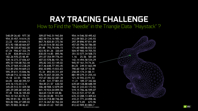
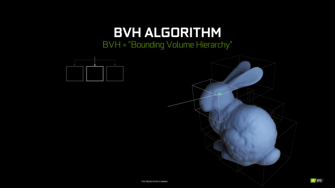
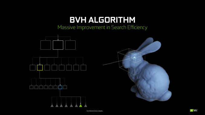
A big part of that hardware, in turn, will go into solving the most basic problem of ray tracing: how do you figure out what a ray is intersecting with? The most common solution to this problem is to store triangles in a data structure that is well-suited for ray tracing. And this data structure is called a Bounding Volume Hierarchy.
Conceptually, a BVH is relatively simple – at least for the purposes of this article. Rather than testing every polygon to see if a ray interacts with it, the idea is to test a portion of a scene to see if it interacts with a ray, and then keep drilling down. If there is an intersection with that portion of the scene, then subdivide it into smaller portions and test again. And again. And again. All the way until you reach the individual polygon, at which point the ray testing is resolved.
For the computer scientists in the crowd, this might sound a lot like an application of a binary search, and it is. Each test allows for a significant number of options (in this case polygons) to be discarded as possible answers. This gets to the right polygon in just a fraction of the time. A BVH, in turn, is stored in what’s essentially a tree data structure, with each subdivision – called bounding boxes – stored as children of their parent bounding box.
Now the catch with BVH is that while it radically cuts down on the amount of ray intersection needed compared to a naïve implementation, it’s still not super cheap. A number of tests are still required for each ray, with both successful and failed tests adding to the total number of tests taken. And all of this is for a single ray, when a significant number of rays are going to be needed for each pixel. Which is why hardware acceleration of the process is so important (and not at all easy).
The other major computational cost here is that BVHs themselves aren’t free. One needs to be created for a scene from the polygons in it, so there is an additional step before ray casting can even begin. This is more a developer concern – when can they modify and reuse a BVH versus building a new one – but it’s another step in the process. Furthermore it’s an example of why developer training and efficient engine implementations are so crucial to the process, as a poor implementation can make ray tracing much too slow to be viable.
The Turing Architecture: Volta in Spirit
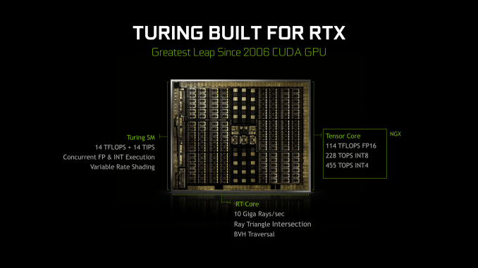
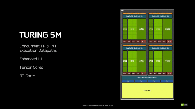
Diving straight into the microarchitecture, the new Turing SM looks very different to the Pascal SM, but those who’ve been keeping track of Volta will notice a lot of similarities to the NVIDIA’s more recent microarchitecture. In fact, on a high-level, the Turing SM is fundamentally the same, with the notable exception of a new IP block: the RT Core. Putting the RT Cores and Tensor Cores aside for now, the most drastic changes from Pascal are same ones that differentiated Volta from Pascal. Turing’s advanced shading features are also in the same bucket in needing explicit developer support.
Like Volta, the Turing SM is partitioned into 4 sub-cores (or processing blocks) with each sub-core having a single warp scheduler and dispatch unit, as opposed Pascal’s 2 partition setup with two dispatch ports per sub-core warp scheduler. There are some fairly major implications with change, and broadly-speaking this means that Volta/Turing loses the capability to issue a second, non-dependent instruction from a thread for a single clock cycle. Turing is presumably identical to Volta performing instructions over two cycles but with schedulers that can issue an independent instruction every cycle, so ultimately Turing can maintain 2-way instruction level parallelism (ILP) this way, while still having twice the amount of schedulers over Pascal.
Like we saw in Volta, these changes go hand-in-hand with the new scheduling/execution model with independent thread scheduling that Turing also has, though differences were not disclosed at this time. Rather than per-warp like Pascal, Volta and Turing have per-thread scheduling resources, with a program counter and stack per-thread to track thread state, as well as a convergence optimizer to intelligently group active same-warp threads together into SIMT units. So all threads are equally concurrent, regardless of warp, and can yield and reconverge.
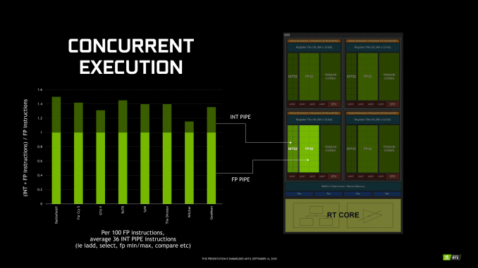
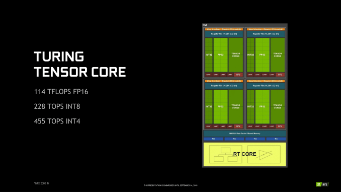
In terms of the CUDA cores and ALUs, the Turing sub-core has 16 INT32 cores, 16 FP32 cores, and 2 Tensor Cores, the same setup as the Volta sub-core. With the split INT/FP datapath model like Volta, Turing can also concurrently execute FP and INT instructions, which as we will see, is much more relevant with the RT cores involved. Where Turing differs is in lacking Volta’s full complement of FP64 cores, instead having a token amount (2 per SM) for compatibility reasons and resulting in FP64 throughput being 1/32 the TFLOP rate of FP32. Maimed FP64 is standard for NVIDIA’s consumer GPUs, but what has not been standard until now is Turing’s full 2x FP16 throughput, which was available in GP100 but was crippled in the other Pascal GPUs.
While these details may be more on the technical side of things, in Volta this design seemed inextricably linked to maximizing the most amount of performance from tensor cores, but minimizing disrupting parallelism or coordination with other compute workloads. The same is most likely true with Turing’s 2nd generation tensor cores and RT cores, where 4 independently scheduled sub-cores and granular thread manipulation would be very useful in extracting the most performance out of mixed gaming-oriented workloads, where rendering a single frame would be pulling in multiple blocks of the GPU to work in conjunction. This is actually a concept that circumscribes the RTX-OPS metric, and we will revisit that in depth later.
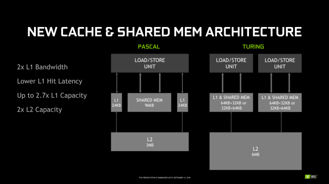
Memory-wise, every sub-core now has an L0 instruction cache like Volta, with identically sized 64 KB register file. In Volta, this was important in reducing latency when the tensor cores were in play, and in Turing this likely benefits RT cores similarly, which we will discuss in a later section. Otherwise, the Turing SM also has 4 load/store units per sub-core, down from 8 in Volta, but still maintains 4 texture units.
Further up the memory hierarchy is the new L1 data cache and Shared Memory (SMEM) that has been revamped and unified into a single partitionable memory block, another Volta innovation. For Turing, this is looking to be a combined 96 KB L1/SMEM, which traditional graphics workloads divide as 64KB for dedicated graphics shader RAM and as 32 KB for texture cache and register file spill area. Meanwhile, compute workloads can partition the L1/SMEM with up to 64 KB as L1 with the remaining 32 KB as SMEM, or vice versa. For Volta, SMEM can be configured up to 96 KB.
Though many of these details are only of value to developers, there are several important points to make here. One is simply how similar Turing and Volta are, as opposed to ; after all, they are in the same generational compute family. Another is how compute-oriented Volta – and by extension, Turing – are, and the fact that this is being brought to consumers as part of NVIDIA’s proclaimed ‘future of gaming.’ Part of that is, of course, permitting fast FP16 in potential gaming workloads, but Turing goes far beyond that. At the low level, Turing is less about maximizing traditional gaming, and more about maximizing gaming with special technologies such as real-time raytracing.
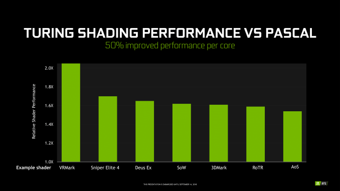
For their part, NVIDIA points to Turing’s leap in performance from Pascal, from memory hierarchy bandwidth uplifts to 50% more shader performance per core, but unfortunately for today we can’t connect this with any real world data or performance. With concurrent FP/INT execution in gaming, the company is keen to point out that around 36 INT instructions could be freed up by moving to its own pipe, which nevertheless doesn’t describe Turing performance, only the applicability of its concurrent execution feature in games.
It becomes a bit of a complex scenario, as we know that Volta already improved on Pascal in these aspects with concurrent execution, a brand new ISA, and reworked SM. And it doesn’t seem to involve architectural changes for significant clockspeed enhancements a la Pascal from Maxwell, though of course on the process side the 12nm FFN is a factor. So it comes down to special gaming workloads and real-world performance. The latter is not available today, but the former is so important to Turing that it merited dropping ‘GTX’ for ‘RTX’. And of those special workloads, real-time raytracing and RT cores take center stage.
Turing RT Cores: Hybrid Rendering and Real Time Raytracing
As it presents itself in Turing, real-time raytracing doesn’t completely replace traditional rasterization-based rendering, instead existing as part of Turing’s ‘hybrid rendering’ model. In other words, rasterization is used for most rendering, while ray-tracing techniques are used for select graphical effects. Meanwhile, the ‘real-time’ performance is generally achieved with a very small amount of rays (e.g. 1 or 2) per pixel, and a very large amount of denoising.
The specific implementation is ultimately in the hands of developers, and NVIDIA naturally has their raytracing development ecosystem, which we’ll go over in a later section. But because of the computational intensity, it simply isn’t possible to use real-time raytracing for the complete rendering workload. And higher resolutions, more complex scenes, and numerous graphical effects also compound the difficulty. So for performance reasons, developers will be utilizing raytracing in a deliberate and targeted manner for specific effects, such as global illumination, ambient occlusion, realistic shadows, reflections, and refractions. Likewise, raytracing may be limited to specific objects in a scene, and rasterization and z-buffering may replace primary ray casting while only secondary rays are raytraced. Thus, the goal of developers is to use raytracing for the most noticeable and realistic effects that rasterization cannot accomplish.
Essentially, this style of ‘hybrid rendering’ is a lot less raytracing than one might imagine from the marketing material. Perhaps a blunt way to generalize might be: real time raytracing in Turing typically means only certain objects are being rendered with certain raytraced graphical effects, using a minimal amount of rays per pixel and/or only raytracing secondary rays, and using a lot of denoising filtering; anything more would affect performance too much. Interestingly, explaining all the caveats this way both undersells and oversells the technology, because therein lies the paradox. Even in this very circumscribed way, GPU performance is significantly affected, but image quality is enhanced with a realism that cannot be provided by a higher resolution or better anti-aliasing. Except ‘real time’ interactivity in gaming essentially means a minimum of 30 to 45 fps, and lowering the render resolution to achieve those framerates hurts image quality. What complicates this is that real time raytracing is indeed considered the ‘holy grail’ of computer graphics, and so managing the feat at all is a big deal, but there are equally valid professional and consumer perspectives on how that translates into a compelling product.
On that note, then, NVIDIA accomplished what the industry was not expecting to be possible for at least a few more years, and certainly not at this scale and development ecosystem. Real time raytracing is the culmination of a decade or so of work, and the Turing RT Cores are the lynchpin. But in building up to it, NVIDIA summarizes the achievement as a result of:
- Hybrid rendering pipeline
- Efficient denoising algorithms
- Efficient BVH algorithms
By themselves, these developments were unable to improve raytracing efficiency, but set the stage for RT Cores. By virtue of raytracing’s importance in the world of computer graphics, NVIDIA Research has been looking into various BVH implementations for quite some time, as well as exploring architectural concerns for raytracing acceleration, something easily noted from their patents and publications. Likewise with denoising, though the latest trend has veered towards using AI and by extension Tensor Cores. When BVH became a standard of sorts, NVIDIA was able to design a corresponding fixed function hardware accelerator.
Being so crucial to their achievement, NVIDIA is not disclosing many details about the RT Cores or their BVH implementation. Of the details given, much is somewhat generic. To reiterate, BVH is a rather general category, and all modern raytracing acceleration structures are typically BVH or kd-tree based.
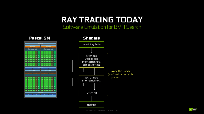
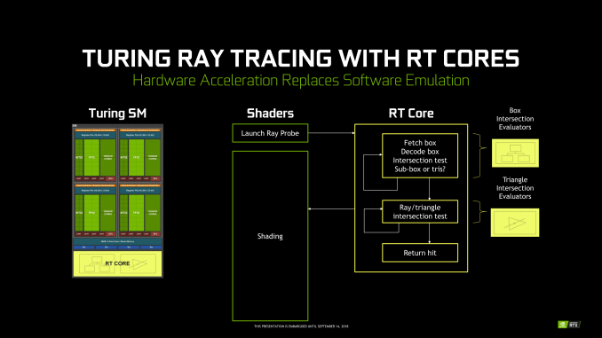
Unlike Tensor Cores, which are better seen as an FMA array alongside the FP and INT cores, the RT Cores are more like a classic offloading IP block. Treated very similar to texture units by the sub-cores, instructions bound for RT Cores are routed out of sub-cores, which is later notified on completion. Upon receiving a ray probe from the SM, the RT Core proceeds to autonomously traverse the BVH and perform ray-intersection tests. This type of ‘traversal and intersection’ fixed function raytracing accelerator is a well-known concept and has had quite a few implementations over the years, as traversal and intersection testing are two of the most computationally intensive tasks involved. In comparison, traversing the BVH in shaders would require thousands of instruction slots per ray cast, all for testing against bounding box intersections in the BVH.
Returning to the RT Core, it will then return any hits and letting shaders do implement the result. The RT Core also handles some grouping and scheduling of memory operations for maximizing memory throughput across multiple rays. And given the workload, presumably some amount of memory and/or ray buffer within the SIP block as well. Like in many other workloads, memory bandwidth is a common bottleneck in raytracing, and has been the focus of several NVIDIA Research papers. And in general, raytracing workloads result in very irregular and random memory accesses, mainly due to incoherent rays, that prove especially problematic for how GPUs typically utilize their memory.
But otherwise, everything else is at a high level governed by the API (i.e. DXR) and the application; construction and update of the BVH is done on CUDA cores, governed by the particular IHV – in this case, NVIDIA – in their DXR implementation.
All-in-all, there’s clearly more involved, and we’ll be looking to run some microbenchmarks in the future. NVIDIA’s custom BVH algorithms are clearly in play, but right now we can’t say what the optimizations might be, such as compressions, wide BVH, node subdivision into treelets. The way the RT Cores are integrated into the SM and into the architecture is likely crucial to how it operates well. Internally, the RT Core might just be a basic traversal and intersection unit, but it might also have other bits inside; one of NVIDIA’s recent patents provide a representation, albeit dated, of what else might be present. I, for one, would not be surprised to see it closely tied with the MIO blocks, and perhaps did more with coherency gathering by manipulating memory traffic for higher efficiency. It would need to coordinate well with the other workloads in the SMs without strangling memory access with unmitigated incoherent rays.
Nevertheless, details like performance impact are as yet unspecified.
Turing Tensor Cores: Leveraging Deep Learning Inference for Gaming
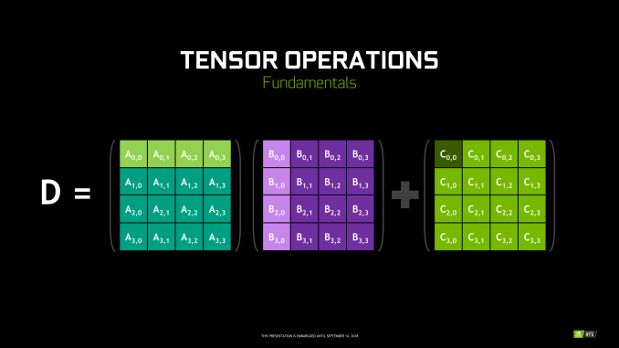
Though RT Cores are Turing’s poster child feature, the tensor cores were very much Volta’s. In Turing, they’ve been updated, reflecting its positioning as a gaming/consumer feature via inferencing. The main changes for the 2nd generation tensor cores are INT8 and INT4 precision modes for inferencing, enabled by new hardware data paths, and perform dot products to accumulate into an INT32 product. INT8 mode operates at double the FP16 rate, or 2048 integer operations per clock. INT4 mode operates at quadruple the FP16 rate, or 4096 integer ops per clock.
Naturally, only some networks tolerate these lower precisions and any necessary quantization, meaning the storage and calculation of compacted format data. INT4 is firmly in the research area, whereas INT8’s practical applicability is much more developed. Regardless, the 2nd generation tensor cores still have FP16 mode, which they now support in a pure FP16 mode without FP32 accumulator. While CUDA 10 is not yet out, the enhanced WMMA operations should shed light on any other differences, such as additional accepted matrix sizes for operands.
Inasmuch as deep learning is involved, NVIDIA is pushing what was a purely compute/professional feature into consumer territory, and we will go over the full picture in a later section. For Turing, the tensor cores can accelerate the features under the NGX umbrella, which includes DLSS. They can also accelerate certain AI-based denoisers that cleanup and correct real time raytraced rendering, though most developers seem to be opting for non-tensor core accelerated denoisers at the moment.
The Turing Trio: TU102, TU104, & TU106
Altogether, NVIDIA will be kicking off the Turing generation with a trio of GPUs: TU102, TU104, and TU106. Notably, this is a much larger product stack than any past NVIDIA consumer launch. Typically NVIDIA releases just a single GPU on launch day – usually the 104 model – and then additional GPUs filter in months down the line as production ramps up. Instead NVIDIA will be releasing products based on two different GPUs this month, and then following that up with a third GPU one month later.
Since all three GPUs are Turing, all three GPUs share the same basic design, and in the same ratios. Meaning that TU104 and TU106 are proportionally cut-down versions of TU102, without any radical changes between the GPUs like we’ve seen between GP100 and GP102/104/106. This also means that TU104 and TU106 are proportionally powerful GPUs; NVIDIA hasn’t stripped TU106’s RT and tensor cores to a bare minimum to save on the transistor count, for example.
| NVIDIA Turing GPU Comparison | ||||||
| TU102 | TU104 | TU106 | GP102 | |||
| CUDA Cores | 4608 | 3072 | 2304 | 3840 | ||
| SMs | 72 | 48 | 36 | 30 | ||
| Texture Units | 288 | 192 | 144 | 240 | ||
| RT Cores | 72 | 48 | 36 | N/A | ||
| Tensor Cores | 576 | 384 | 288 | N/A | ||
| ROPs | 96 | 64 | 64 | 96 | ||
| Memory Bus Width | 384-bit | 256-bit | 256-bit | 384-bit | ||
| L2 Cache | 6MB | 4MB | 4MB | 3MB | ||
| Register File (Total) | 18MB | 12MB | 9MB | 7.5MB | ||
| Architecture | Turing | Turing | Turing | Pascal | ||
| Manufacturing Process | TSMC 12nm "FFN" | TSMC 12nm "FFN" | TSMC 12nm "FFN" | TSMC 16nm | ||
| Die Size | 754mm2 | 545mm2 | 445mm2 | 471mm2 | ||
The flagship for the Turing family is a part that we’ve quickly become familiar with, and that is TU102. The largest of the Turing GPUs, this is the GPU NVIDIA is tapping for two of their new Quadro RTX cards, as well as the GeForce RTX 2080 Ti.
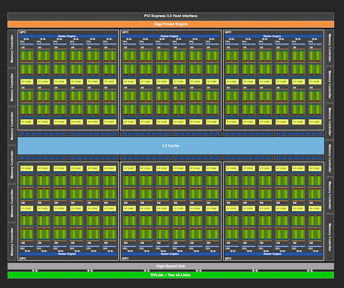
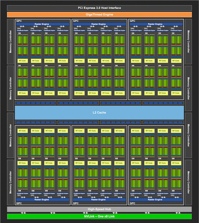
A fully-enabled TU102 is comprised of 72 SMs, organized into 6 GPCs. And since the number of RT cores and tensor cores is proportional to the SM count, we’re looking at 72 RT cores and 576 tensor cores. Paired with this harder is 12 ROP/memory controller partitions, giving the GPU a native 384-bit memory bus and 96 ROPs for pixel blending.
Relative to NVIDIA’s GV100 GPU, TU102 is smaller and contains fewer SM and tensor cores, but the difference is not quite as great as you might think. The 18.6B transistor, 754mm2 chip still packs 85% of GV100’s common hardware even with its physically small size, and then this value doesn’t include all the die space taking up by Turing’s new features such as the RT cores and the newer generation tensor cores. So this is still an incredibly big chip, and is especially notable since NVIDIA will be putting it in a consumer card.
Outside of the standard Turing graphics hardware, of particular note here is that because TU102 pulls double-duty with high-end Quadro cards, it’s the only GPU to feature two NVLink connections. Each NVLink connection – which NVIDIA technically classifies as an 8x NVlink – is capable of offering 25GB/sec of bandwidth in each direction, for a total of 50GB/sec of bandwidth in each direction when the links are used in aggregate.
The middle child of the stack and the traditional frontrunner in NVIDIA’s GPU release cadence is the TU104. This part is a smaller, slimmer Turing GPU that shaves off some SMs in the name of coming in at a smaller die size. Altogether it offers 48 SMs and 8 ROP/MC partitions, making it roughly two-thirds of a TP102.
In exchange the chip is also notably smaller. Not small by any means, but smaller. The part comes in at 13.6B transistors, which are laid out in a 545mm2 die. This still makes it the largest x04 chip by a landslide, coming in much larger than even the late-generation 28nm GM204 in 2014. Still, NVIDIA shaved off over 200mm2 relative to TU102, so there are significant die savings here compared to using an actual cut-down TU102.
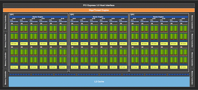
The TU104 will be going into just one consumer card, at least for now. This is the GeForce RTX 2080. It will also be going into its Quadro counterpart, the Quadro RTX 5000. Notably, only the Quadro is getting a fully enabled chip, while RTX 2080 ships with a couple of disabled SMs. This GPU also features NVLink support, but this time it’s a single x8 link, half of what TU102 offered.
Finally, rounding out the trio is the mysterious TU106 GPU, which prior to today had not been disclosed by NVIDIA. Rather than using a cut-down TU104 in the GeForce RTX 2070, they’re going to use an entirely different GPU.
TU106 in turn is a smaller chip than TU104, but perhaps not as much as you think. NVIDIA is still including 36 SMs and the same 8 ROP/MC partitions, so in terms of pixel throughput and bandwidth TU106 is actually identical to TU104 on paper. It’s only when looking at the processor elements that we see that we’ve ended up with what’s essentially 75% of a TU104. On which note however, it’s rather interesting that NVIDIA opted to halve the GPC count here; TU106 packs 12 SMs to a GPC, versus 8 to a GPC in TU104.
The payoff for NVIDIA here is that TU106 once again brings down NVIDIA’s large die sizes. The chip features 10.8 billion transistors, which at 445mm2 still makes it a beefy chip. But this is at least finally smaller than the GP102 used in the Pascal Titan Xp cards.
The net result of all of this is that NVIDIA has a very interesting GPU launch stack, one unlike anything we’ve seen before. No two GeForce cards share the same GPU; there is a GPU for each and every card right now. And we’re seeing NVIDIA launch two GPUs right out the door, including the massive TU102, with the TU106 to follow close behind. So it’s a very different setup than the norm for NVIDIA.
Turing In Practice: GeForce RTX 2080 Ti, 2080, & 2070
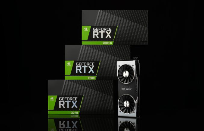
These 3 GPUs, in turn, form the foundation of the GeForce RTX 2080 Ti, RTX 2080, and RTX 2070. As previously announced by NVIDIA, the first two cards will go on sale next week, on September 20th. Meanwhile the RTX 2070 will ship a bit later, with sales starting in October.
We’ll be giving the RTX 2080 Ti and RTX 2080 a full work-through next week in our review of those cards. In the meantime, here’s a recap of their specifications and pricing.
| NVIDIA GeForce x80 Ti Specification Comparison | ||||||
| RTX 2080 Ti Founder's Edition |
RTX 2080 Ti | GTX 1080 Ti | GTX 980 Ti | |||
| CUDA Cores | 4352 | 4352 | 3584 | 2816 | ||
| ROPs | 88 | 88 | 88 | 96 | ||
| Core Clock | 1350MHz | 1350MHz | 1481MHz | 1000MHz | ||
| Boost Clock | 1635MHz | 1545MHz | 1582MHz | 1075MHz | ||
| Memory Clock | 14Gbps GDDR6 | 14Gbps GDDR6 | 11Gbps GDDR5X | 7Gbps GDDR5 | ||
| Memory Bus Width | 352-bit | 352-bit | 352-bit | 384-bit | ||
| VRAM | 11GB | 11GB | 11GB | 6GB | ||
| Single Precision Perf. | 14.2 TFLOPs | 13.4 TFLOPs | 11.3 TFLOPs | 6.1 TFLOPs | ||
| "RTX-OPS" | 78T | 78T | N/A | N/A | ||
| TDP | 260W | 250W | 250W | 250W | ||
| GPU | TU102 | TU102 | GP102 | GM200 | ||
| Architecture | Turing | Turing | Pascal | Maxwell | ||
| Manufacturing Process | TSMC 12nm "FFN" | TSMC 12nm "FFN" | TSMC 16nm | TSMC 28nm | ||
| Launch Date | 09/20/2018 | 09/20/2018 | 03/10/2017 | 06/01/2015 | ||
| Launch Price | $1199 | $999 | MSRP: $699 Founders: $699 |
$649 | ||
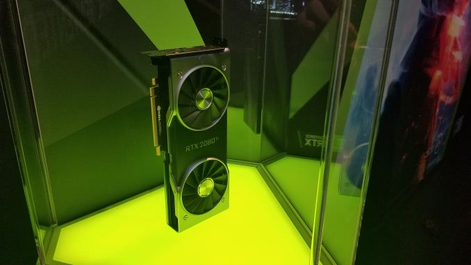
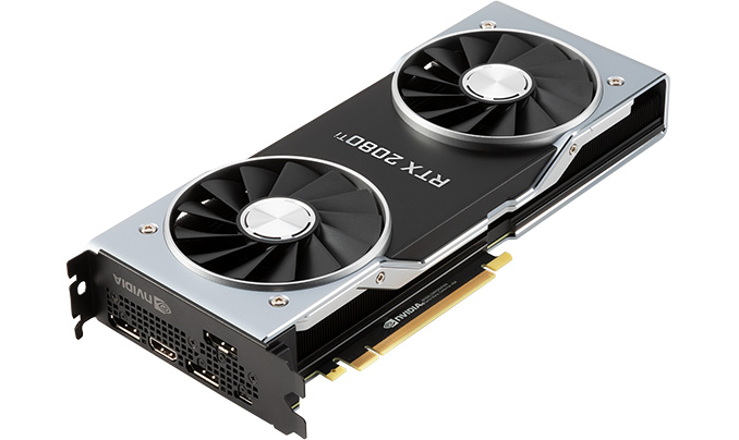
The king of NVIDIA’s new product stack, the GeForce RTX 2080 Ti is without a doubt an interesting card. NVIDIA’s consumer flagship sports 4352 Turing CUDA cores and 544 tensor cores, as well as 68 RT cores. Like its Quadro counterpart, this card is rated for 10 GigaRays/second, and for traditional compute we’re looking at 13.4 TFLOPS based on these specifications. Note that on paper this is only 19% higher than GTX 1080 Ti, which is why NVIDIA’s architectural changes and efficiency improvements are going to carry the day here, rather than brute forcing the matter with more hardware.
Clockspeeds have actually dropped from generation to generation here. Whereas the GTX 1080 Ti started at 1.48GHz and had an official boost clock rating of 1.58GHz (and in practice boosting higher still), RTX 2080 Ti starts at 1.35GHz and boosts to 1.55GHz, while we don’t know anything about the practical boost limits. So assuming NVIDIA is being as equally conservative as the last generation, then this means the average clockspeeds have dropped slightly.
Moving on, for the ROP and memory subsystem we’re looking at a partially-enabled configuration here as well. RTX 2080 Ti offers 88 of 96 ROPs, which is a result of NVIDIA disabling one of the 12 ROP/MC partitions. Even then, relative to the GTX 1080 Ti and thanks to GDDR6, memory clockspeeds have been boosted from 11Gbps to 14Gbps, a 27% increase. And since the memory bus width itself remains identical at 352-bits wide, this means the final memory bandwidth increase is also 27%.
Past this, things start diverging a bit. NVIDIA is once again offering their reference-grade Founders Edition cards, and unlike with the GeForce 10 series, the 20 series FE cards have slightly different specifications than their base specification compatriots. Specifically, NVIDIA has cranked up the clockspeed and the resulting TDP a bit, giving the 2080 Ti FE an on-paper 6% performance advantage, and also a 10W higher TDP. For the standard cards then, the TDP is the x80 Ti-traditional 250W, while the FE card moves to 260W.
| NVIDIA GeForce x80 Specification Comparison | ||||||
| RTX 2080 Founder's Edition |
RTX 2080 | GTX 1080 | GTX 980 | |||
| CUDA Cores | 2944 | 2944 | 2560 | 2048 | ||
| ROPs | 64 | 64 | 64 | 64 | ||
| Core Clock | 1515MHz | 1515MHz | 1607MHz | 1126MHz | ||
| Boost Clock | 1800MHz | 1710MHz | 1733MHz | 1216MHz | ||
| Memory Clock | 14Gbps GDDR6 | 14Gbps GDDR6 | 10Gbps GDDR5X | 7Gbps GDDR5 | ||
| Memory Bus Width | 256-bit | 256-bit | 256-bit | 256-bit | ||
| VRAM | 8GB | 8GB | 8GB | 4GB | ||
| Single Precision Perf. | 10.6 TFLOPs | 10.1 TFLOPs | 8.9 TFLOPs | 5.0 TFLOPs | ||
| "RTX-OPS" | 60T | 60T | N/A | N/A | ||
| TDP | 225W | 215W | 180W | 165W | ||
| GPU | TU104 | TU104 | GP104 | GM204 | ||
| Architecture | Turing | Turing | Pascal | Maxwell | ||
| Manufacturing Process | TSMC 12nm "FFN" | TSMC 12nm "FFN" | TSMC 16nm | TSMC 28nm | ||
| Launch Date | 09/20/2018 | 09/20/2018 | 05/27/2016 | 09/18/2014 | ||
| Launch Price | $799 | $699 | MSRP: $599 Founders $699 |
$549 | ||
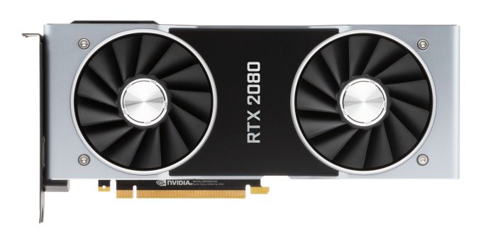
Moving down the line, we have the GeForce RTX 2080. Based on TU104, this card offers 2944 CUDA cores paired with 368 tensor cores. Like the RTX 1080 Ti, clockspeeds have dropped a bit from generation to generation, as the base clock is down to 1515MHz and the boost clock to 1710MHz. All told we’re looking at a pure CUDA core compute throughput of 10.1 TFLOPs, about 13% higher than the GTX 1080. Or if we compare it to the RTX 2080 Ti, we’d see around 75% of the expected compute/tensor performance, which is only a bit larger than the jump we saw between the GTX 1080 and GTX 1080 Ti.
Meanwhile the card does come with a fully enabled memory bus, meaning we’re looking at 8GB of GDDR6 running at 14Gbps, on top of a 256-bit memory bus. Relative to the GTX 1080 this is an even more significant 40% increase in memory bandwidth.
As for TDPs, they’ve gone up for this band of cards. The stock RTX 2080 will have a 215W TDP, up 30W from the GTX 1080’s 180W TDP, and an even bigger increase if we look at GTX 980’s 165W TDP. It’s no secret that NVIDIA is fighting a losing battle with Moore’s Law here, and barring massive efficiency improvements, there is a need to increase TDPs to keep up overall performance. TU104 is a big chip, and without a full node shrink, it would seem that NVIDIA has to pay a power penalty instead. In the meantime this higher TDP also negates some of the RTX 2080 Ti’s power disadvantage, as now that gap is just 35W instead of 65W.
| NVIDIA GeForce x70 Specification Comparison | ||||||
| RTX 2070 Founder's Edition |
RTX 2070 | GTX 1070 | GTX 970 | |||
| CUDA Cores | 2304 | 2304 | 1920 | 1664 | ||
| ROPs | 64 | 64 | 64 | 64 | ||
| Core Clock | 1410MHz | 1410MHz | 1506MHz | 1050MHz | ||
| Boost Clock | 1710MHz | 1620MHz | 1683MHz | 1178MHz | ||
| Memory Clock | 14Gbps GDDR6 | 14Gbps GDDR6 | 8Gbps GDDR5 | 7Gbps GDDR5 | ||
| Memory Bus Width | 256-bit | 256-bit | 256-bit | 256-bit | ||
| VRAM | 8GB | 8GB | 8GB | 4GB | ||
| Single Precision Perf. | 7.9 TFLOPs | 7.5 TFLOPs | 6.5 TFLOPs | 3.9 TFLOPs | ||
| "RTX-OPS" | 45T | 45T | N/A | N/A | ||
| TDP | 185W | 175W | 150W | 145W | ||
| GPU | TU106 | TU106 | GP104 | GM204 | ||
| Architecture | Turing | Turing | Pascal | Maxwell | ||
| Manufacturing Process | TSMC 12nm "FFN" | TSMC 12nm "FFN" | TSMC 16nm | TSMC 28nm | ||
| Launch Date | 09/20/2018 | 09/20/2018 | 06/10/2016 | 09/18/2014 | ||
| Launch Price | $599 | $499 | MSRP: $379 Founders $449 |
$329 | ||
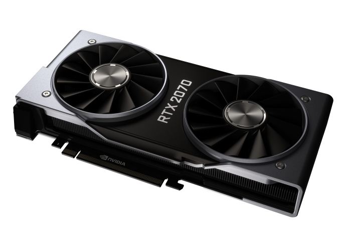
The final member of the new GeForce RTX family is the GeForce RTX 2070. Traditional for its roots, this is the “value” enthusiast card, giving up some of the RTX 2080’s performance in exchange for a lower price. Though with prices starting at $499, “value” and “cheap” are not the same thing.
With TU106, NVIDIA has shaved off a number of SMs. The end result is that the RTX 2070 offers 2304 CUDA cores and 288 tensor cores. Meanwhile ray tracing performance is rated at 6 GigaRays/second. Meanwhile in an interesting twist, this is the only consumer part launching with a fully-enabled GPU: TU106 offers 36 SMs, and NVIDIA is using all 36 of them.
Like the other RTX cards, clockspeeds have dropped a bit versus the previous generation; the base clock now starts at 1410MHz, and the boost clock is 1620MHz. On paper then, compute throughput works out to 7.5 TFLOPs, up 15% from GTX 1070. Or if we compare it to the 2080, the 2070 should deliver around 75% of its bigger sibling’s compute performance, which makes the jumps between the 2070, 2080, and 2080 Ti all very symmetrical. This is also an ever so slightly smaller gap than what was between the GTX 1080 and GTX 1070.
Also like the RTX 2080, this appears to be a fully enabled memory configuration. Meaning we’re looking at 8GB of GDDR6 running at 14Gbps, on top of a 256-bit memory bus. Relative to the GTX 1070 this is the single greatest bandwidth increase of all of the RTX cards; the 2070 will enjoy a 75% increase in memory bandwidth over its Pascal predecessor, as the GTX 1070 never did use GDDR5X.
TDPs have gone up here as well. The RTX 2070 is rated for 175W, up from 150W for the GTX 1070, and 145W for the GTX 970. As with the RTX 2080, it looks like NVIDIA is paying for their performance and new features via higher power consumption in lieu of a full node shrink.
Feeding the Beast (2018): GDDR6 & Memory Compression
Memory bandwidth has always been a challenge for video cards, and that challenge only continues to get harder. Thanks to the mechanics of Moore’s Law, GPU transistor counts – and therefore the quantities of various cores – is growing at a rapid pace. Meanwhile DRAM, whose bandwidth is not subject to the same laws, has grown at a much smaller pace.
The net result is that with nearly every generation, the amount of memory bandwidth available per FLOP, per texture lookup, and per pixel blend has continued to drop. So to keep GPU performance scaling – to feed the great graphical beast – GPU manufacturers and the memory industry as a whole have to look for new ways to boost memory bandwidth for future memory technologies while reducing the amount of memory bandwidth they’re using right now. Neither is easy, and both are areas where NVIDIA has been executing well on over most of the past decade, making it an architectural strength for the company.
| NVIDIA Memory Bandwidth per FLOP (In Bits) | ||||||
| GPU | Bandwidth/FLOP | Total CUDA FLOPs | Total Bandwidth | |||
| RTX 2080 | 0.36 bits | 10.06 TFLOPs | 448GB/sec | |||
| GTX 1080 | 0.29 bits | 8.87 TFLOPs | 320GB/sec | |||
| GTX 980 | 0.36 bits | 4.98 TFLOPs | 224GB/sec | |||
| GTX 680 | 0.47 bits | 3.25 TFLOPs | 192GB/sec | |||
| GTX 580 | 0.97 bits | 1.58 TFLOPs | 192GB/sec | |||
Turing, in turn, is a bit of an interesting swerve in this pattern thanks to its heavy focus on ray tracing and neural network inferencing. If we're looking at memory bandwidth merely per CUDA core FLOP, then bandwidth per FLOP has actually gone up, since RTX 2080 doesn't deliver a significant increase in (on-paper) CUDA core throughput relative to GTX 1080. However RTX 2080 also now has to feed ray tracing cores and tensor cores, both of which are very bandwidth hungry on their own. So while in pure, FP32 core compute scenarios the situation has improved a bit, once the entire GPU is put to work, the amount of contention for memory bandwidth is still higher than ever.
In terms of memory technologies, the 16nm/14nm generation of GPUs saw an interesting and atypical divergence in the memory space. GDDR5, which has been with us for a decade now, has been ripe for replacement. The JEDEC, the industry standardization body responsible for setting common memory standards, initially approached this in two directions. The first route was more traditional, developing a successor technology to GDDR5, which became GDDR5X. Meanwhile the more radical approach was ultra-wide I/O technologies, which became the High Bandwidth Memory (HBM) standards.
NVIDIA for their part embraced both, but at different levels. HBM is very powerful, but the realities of wide I/O make it harder to manufacture and more costly to put on a product, thanks to the need for a silicon interposer. As a result, HBM (and specifically, HBM2) has only ever been used on NVIDIA’s flagship compute GPUs, the GP100 and GV100. For everything else, NVIDIA turned to GDDR5X. And this is where things get a bit odd.
GDDR5X is a JEDEC standard like GDDR5 before it, but it simply never saw the same kind of adoption that GDDR5 did. This goes both for memory vendors and GPU vendors. Only Micron ever produced the memory, and only NVIDIA ever used it. So the fastest Pascal cards – GTX 1080, GTX 1080 Ti, & Titan Xp – are outliers in that they’re the only (consumer) cards using this memory technology. GDDR5X was an important piece of the Pascal puzzle as it allowed NVIDIA to better feed their fastest cards, but in time it has essentially became a dead-end branch of GDDR memory technology as it never saw the kind of adoption required to reach critical mass.
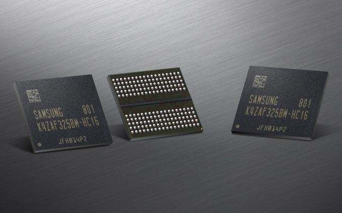
So where did GDDR branch to instead? This brings us to GDDR6, the latest and greatest in GDDR memory technology. And unlike GDDR5X before it, GDDR6 has the full backing of the Big 3 memory manufacturers – Samsung, SK Hynix, and Micron – so the memory industry as a whole has a much larger stake in the technology. For NVIDIA’s products, this is evident right off the bat: NVIDIA is using Samsung’s 16Gb capacity GDDR6 modules for their Quadro cards, and meanwhile they’re tapping Micron’s 8Gb modules for the new GeForce RTX cards.
The performance impact of GDDR6, in turn, depends in part on what we’re comparing it to. Relative to GDDR5X, GDDR6 is not quite as big of a step up as some past memory generations, as many of GDDR6’s innovations were already baked into GDDR5X. GDDR5 officially topped out at 8Gbps per pin (with NV working with partners to do 9Gbps overclocked SKUs), while NVIDIA shipped GDDR5X cards clocked as high as 11.4Gbps. GDDR6, in turn, is going to be starting at 14Gbps in graphics cards, with future generations of the technology set to reach 16Gbps and higher. So for the likes of NVIDIA’s x70 cards, the switch from GDDR5 to GDDR6 is going to be one of those massive once-in-a-generation bandwidth jumps. However for NVIDIA’s x80 cards, the upgrade from GDDR5X to GDDR6 is going to give those products a healthy increase in memory bandwidth, it just won’t be a huge jump.
Diving a bit deeper here, there are really two core changes coming from GDDR5 that enable GDDR6’s big bandwidth boost. The first is the implementation of Quad Data Rate (QDR) signaling on the memory bus. Whereas GDDR5’s memory bus would transfer data twice per write clock (WCK) via DDR, GDDR6 (& 5X) extends this to four transfers per clock. All other things held equal, this allows GDDR6 to transfer twice as much data per clock as GDDR5.
The challenge in doing this, of course, is that the more you pump a memory bus, the tighter the signal integrity requirements. So while it’s simple to say “let’s just double the memory bus bandwidth”, doing it is another matter. In practice a lot of work goes into the GPU memory controller, the memory itself, and the PCB to handle these transmission speeds.
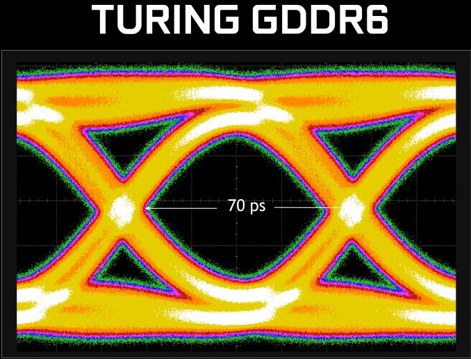
Every time NVIDIA launches support for a new memory technology, they like to roll out a new “eye diagram” signal analysis graph. And while at a high level these things don’t tell us anything we don’t already know – that NVIDIA has the technology working, and that, if it wasn’t, they wouldn’t publish these – they’re none the less neat to see. In this case we’re looking at a fairly clean eye diagram, illustrating the very tight 70ps transitions between data transfers. NVIDIA says that they were able to reduce signal crosstalk by 40% here, which is one of the key signal integrity changes required to make GDDR6’s high speed signaling possible.
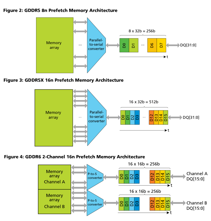
Moving on, the second big change for GDDR6 is that how data is read out of the DRAM cells themselves has changed. For many generations the solution has been to just read and write in larger strides – the prefetch value – with GDDR5 taking this to 8n and GDDR5X taking it to 16n. However the resulting access granularities of 32 bytes and 64 bytes respectively were on the path of becoming increasingly suboptimal for small memory operations. As a result, GDDR6 does a larger prefetch and yet it does not.
Whereas both GDDR5 and GDDR5X used a single 32-bit channel per chip, GDDR6 instead uses a pair of 16-bit channels. This means that in a single memory core clock cycle (ed: not to be confused with the memory bus), 32 bytes will be fetched from each channel for a total of 64 bytes. This means that each GDDR6 memory chip can fetch twice as much data per clock as a GDDR5 chip, but it doesn’t have to be one contiguous chunk of memory. In essence, each GDDR6 memory chip can function like two chips.
For graphics this doesn’t have much of an impact since GPUs already read and write to RAM in massive sequential parallelism. However it’s a more meaningful change for other markets. In this case the smaller memory channels will help with random access performance, especially compared to GDDR5X and its massive 64 byte access granularity.
Moving on, GDDR6 also implements some changes to further reduce power consumption – or perhaps it’s better to say that these keep power consumption from continuing to grow. The standard operating voltage for the memory technology is 1.35v; this is identical to GDDR5X’s 1.35v voltage, but down from 1.5v for standard GDDR5.
The actual power savings are a bit hard to quantify here, as NVIDIA has rolled that data into all of their memory controller optimizations. But at least publicly, what they are saying is that in conjunction with “extensive” clock gating, they’ve been able to improve power efficiency by 20% over Pascal and GDDR5X, and undoubtedly by more versus Pascal paired with GDDR5. That said, these numbers should be taken with a small grain of salt, as these numbers appear to be averages rather than peaks. NVIDIA’s clock gating enhancements are primarily about reducing power consumption when GDDR6 is not running at full utilization, so peak power may be another story.
| GPU Memory Math: GDDR6 vs. HBM2 vs. GDDR5X | ||||||||
| NVIDIA GeForce RTX 2080 Ti (GDDR6) |
NVIDIA GeForce RTX 2080 (GDDR6) |
NVIDIA Titan V (HBM2) |
NVIDIA Titan Xp |
NVIDIA GeForce GTX 1080 Ti | NVIDIA GeForce GTX 1080 | |||
| Total Capacity | 11 GB | 8 GB | 12 GB | 12 GB | 11 GB | 8 GB | ||
| B/W Per Pin | 14 Gb/s | 1.7 Gb/s | 11.4 Gbps | 11 Gbps | ||||
| Chip capacity | 1 GB (8 Gb) | 4 GB (32 Gb) | 1 GB (8 Gb) | |||||
| No. Chips/KGSDs | 11 | 8 | 3 | 12 | 11 | 8 | ||
| B/W Per Chip/Stack | 56 GB/s | 217.6 GB/s | 45.6 GB/s | 44 GB/s | ||||
| Bus Width | 352-bit | 256-bit | 3092-bit | 384-bit | 352-bit | 256-bit | ||
| Total B/W | 616 GB/s | 448GB/s | 652.8 GB/s | 547.7 GB/s | 484 GB/s | 352 GB/s | ||
| DRAM Voltage | 1.35 V | 1.2 V (?) | 1.35 V | |||||
All told then, NVIDIA will be the first GPU manufacturer to roll out GDDR6 support. And with the GTX 2070 on-up having all been announced already, it’s already going to be a wider roll-out than what we saw for GDDR5X. And to put things in numbers, relative to the GTX 10 series, the RTX 2080 Ti will get 27% more memory bandwidth, the RTX 2080 40% more bandwidth, and the RTX 2070 a whopping 75% more memory bandwidth than its predecessor.
However as this is a brand-new memory technology, I’m not sure whether we’re going to see it on the obligatory 2060 & 2050 cards. In transition periods, these tiers have been known to use older memory for cost and supply reasons – so we’ll have to see what happens.
Finally, just as GDDR6 is already seeing greater adoption on the memory manufacturer side, I’m expecting the same on the GPU side. AMD hasn’t announced their plans thus far, but I will be greatly surprised if we see them skip out on GDDR6 like they did GDDR5X.
Turing: Memory Compression Iterated
As I stated at the start of this section, the key to improving GPUs is to tackle the problem from two directions: increase the available memory bandwidth, and then decrease how much of it you use. For the latter, NVIDIA has employed a number of tricks over the years. Perhaps the most potent of which (that they’re willing to talk about, at least) being their memory compression technology.
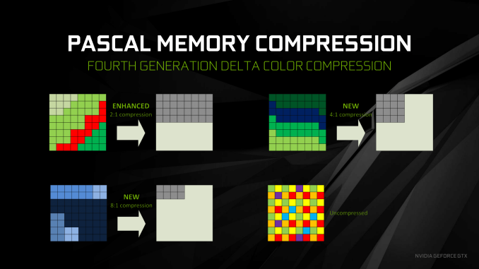
The cornerstone of memory compression is what is called data color compression. DCC is a per-buffer/per-frame compression method that breaks down a frame into tiles, and then looks at the differences between neighboring pixels – their deltas. By utilizing a large pattern library, NVIDIA is able to try different patterns to describe these deltas in as few pixels as possible, ultimately conserving bandwidth throughout the GPU, not only reducing DRAM bandwidth needs, but also L2 bandwidth needs and texture unit bandwidth needs (in the case of reading back a compressed render target).
With Pascal, NVIDIA rolled out their 4th generation technology, and now with Turing we’re at the 5th generation. Unfortunately, details on what the 5th generation entails are very slim; NVIDIA just isn’t talking about the technology much. The nature of DCC is such that it’s meant to be expandable: more silicon can be devoted to allowing more patterns to be checked at once. So it’s practically guaranteed that NVIDIA has once again expanded their library of patterns. However what those expanded patterns are, we don’t know.
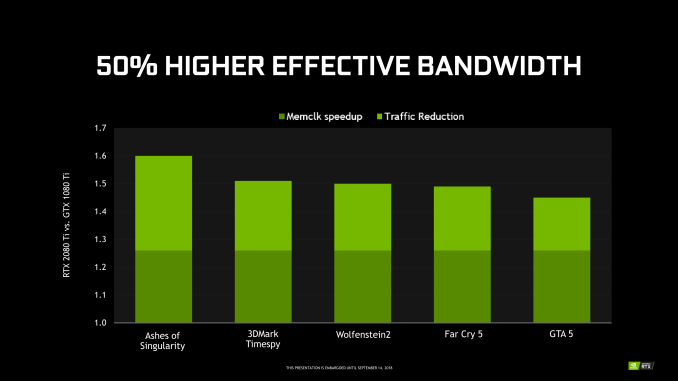
However of the limited information NVIDIA has released, they’ve offered some effective memory bandwidth graphs, with the results broken down into how much of that gain came from actual memory bandwidth increases, and then how much of that came from efficiency increases. In NVIDIA’s examples the effective increase in bandwidth varies by game; as this is the RTX 2080 Ti, GDDR6 provides a constant 27% of the improvement, while the rest of the improvement is variable based on how useful NVIDIA’s memory compression updates are to the given game.
Overall, NVIDIA is seeing anywhere between a 45% increase in effective memory bandwidth for Grand Theft Auto V, up to a 60% increase for Ashes of the Singularity. Which, if we subtract out the base 27% memory clock increase, means that the efficiency increases are between 18% and 33%.
More broadly speaking, NVIDIA is claiming a 50% increase in effective memory bandwidth for the RTX 2080 Ti versus the GTX 1080 Ti. Which again subtracting the base 27% memory bandwidth increase from GDDR6, leaves us with an average efficiency improvement of 23%.
Relative to Pascal then, this is a smaller increase in effective memory bandwidth, but a slightly larger increase in compression efficiency. For Pascal – and specifically, GTX 1080 – NVIDIA claimed a 70% effective memory bandwidth increase, of which 20% was compression improvements.
So while NVIDIA isn’t gaining as much effective memory bandwidth this time around due to the smaller step up from GDDR5X to GDDR6, their compression gains have actually improved a bit between generations. Which is actually a bit surprising, as I would have otherwise expected diminishing returns in the gains from memory compression. After all, NVIDIA started with the most commonly seen pixel patterns, and each generation of DCC would be adding less common patterns.
Unpacking 'RTX', 'NGX', and Game Support
One of the more complicated aspects of GeForce RTX and Turing is not only the 'RTX' branding, but how all of Turing's features are collectively called the NVIDIA RTX platform. To recap, here is a quick list of the separate but similarly named groupings:
- NVIDIA RTX Platform - general platform encompassing all Turing features, including advanced shaders
- NVIDIA RTX Raytracing technology - name for ray tracing technology under RTX platform
- GameWorks Raytracing - raytracing denoiser module for GameWorks SDK
- GeForce RTX - the brand connected with games using NVIDIA RTX real time ray tracing
- GeForce RTX - the brand for graphics cards
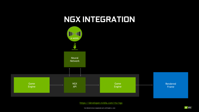
For NGX, it technically falls under the RTX platform, and includes Deep Learning Super Sampling (DLSS). Using a deep neural network (DNN) specific to the game and trained on super high quality 64x supersampled images, or 'ground truth' images, DLSS uses tensor cores to infer high quality antialiased results. In the standard mode, DLSS renders at a lower input sample count, typically 2x less but may depend on the game, and then infers a result, which at target resolution is similar quality to TAA result. A DLSS 2X mode exists, where the input is rendered at the final target resolution and then combined with a larger DLSS network.
Fortunately, GFE is not required for NGX features to work, and all the necessary NGX files will be available via the standard Game Ready drivers, though it's not clear how often DNNs for particular games would be updated.
In the case of RTX-OPS, it describes a workload for a frame where both RT and Tensor Cores are utilized; currently, the classic scenario would be with a game with real time ray tracing and DLSS. So by definition, it only accurately measures that type of workload. However, this metric currently does not apply to any game, as DXR has not yet released. For the time being, the metric does not describe performance any publicly available game.
In sum, then the upcoming game support aligns with the following table.
| Planned NVIDIA Turing Feature Support for Games | |||||
| Game | Real Time Raytracing | Deep Learning Supersampling (DLSS) | Turing Advanced Shading | ||
| Ark: Survival Evolved | Yes | ||||
| Assetto Corsa Competizione | Yes | ||||
| Atomic Heart | Yes | Yes | |||
| Battlefield V | Yes | ||||
| Control | Yes | ||||
| Dauntless | Yes | ||||
| Darksiders III | Yes | ||||
| Deliver Us The Moon: Fortuna | Yes | ||||
| Enlisted | Yes | ||||
| Fear The Wolves | Yes | ||||
| Final Fantasy XV | Yes | ||||
| Fractured Lands | Yes | ||||
| Hellblade: Senua's Sacrifice | Yes | ||||
| Hitman 2 | Yes | ||||
| In Death | Yes | ||||
| Islands of Nyne | Yes | ||||
| Justice | Yes | Yes | |||
| JX3 | Yes | Yes | |||
| KINETIK | Yes | ||||
| MechWarrior 5: Mercenaries | Yes | Yes | |||
| Metro Exodus | Yes | ||||
| Outpost Zero | Yes | ||||
| Overkill's The Walking Dead | Yes | ||||
| PlayerUnknown Battlegrounds | Yes | ||||
| ProjectDH | Yes | ||||
| Remnant: From the Ashes | Yes | ||||
| SCUM | Yes | ||||
| Serious Sam 4: Planet Badass | Yes | ||||
| Shadow of the Tomb Raider | Yes | ||||
| Stormdivers | Yes | ||||
| The Forge Arena | Yes | ||||
| We Happy Few | Yes | ||||
| Wolfenstein II | Yes | ||||
Closing Thoughts
With a tagline like ‘Graphics Reinvented’, NVIDIA is certainly not straying from putting Turing in the most revolutionary limelight as possible. In that sense, NVIDIA is choosing to compare Turing to Pascal rather than Volta for every possible circumstance, especially for gaming. This decision is certainly not unfounded because for consumers, the Turing-based GeForce 20-series succeeds the Pascal-based GeForce 10-series. However, this can give the impression that because Turing is so different from Pascal, it warrants dissimilar comparisons like RTX-OPS metrics or gaming performance uplifts with DLSS or raytracing enabled.
The situation becomes a little more muddled because of several reasons:
- The pricing and availability of the RTX 20-series means that on a purely market segmentation level, it does not directly replace Pascal gaming products
- As gaming-focused cards, the major new features (RT cores, tensor cores, advanced shading) of the RTX 20-series do not operate out-of-the-box in games, are specific to select games, and
- The burden of communication is on the developers to educate consumers on the details of specific raytracing effects or use of AI-accelerated denoisers
These aren’t points that necessarily need to define Turing, except that NVIDIA has pushed the envelope by going all-in with marketing and branding. For their part, NVIDIA will have an continously updated list of games with RTX platform support.
On one hand, Turing seems like a possible solution to the gaming/compute architecture divergence. It seems less likely now that NVIDIA would backtrack into a more standard design for maximum rasterization performance, though obviously that remains to be seen with how the product fares. In any case, as most silicon design firms hvae leapfrogging design teams, the major decisions are likely not to move too far to the fixed function side, if only because the greatest strength of GPUs in compute is its programmability and versatility.
Looking back at ray tracing, it seems that even if it isn't immediately practical, there would still be a seeding effect to be gained via enthusiasts and certain gamers, which would work well with higher-profile AAA games. As we move into next week, it appears that the GeForce RTX 20-series is definitely one of the more nuanced graphics products, with both caveats and potential.

