The AMD Vega GPU Architecture Teaser: Higher IPC, Tiling, & More, Coming in H1’2017
by Ryan Smith on January 5, 2017 9:00 AM ESTHBM2 & “The World’s Most Scalable GPU Memory Architecture”
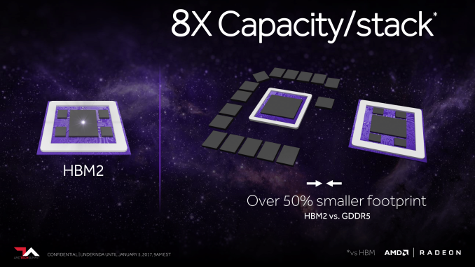
With the launch of the Fiji GPU and resulting Radeon R9 Fury products in 2015, AMD became the first GPU manufacturer to ship with first-generation High Bandwidth Memory (HBM). The ultra-wide memory standard essentially turned the usual rules of GPU memory on its head, replacing narrow, high clocked memory (GDDR5) with wide, low clocked memory. By taking advantage of Through Silicon Vias (TSVs) and silicon interposers, HBM could offer far more bandwidth than GDDR5 while consuming less power and taking up less space.
Now for Vega, AMD is back again with support for the next generation of HBM technology, HBM2. In fact this is the very first thing we ever learned about Vega, going back to AMD’s roadmap from last year where it was the sole detail listed for the architecture.
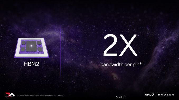
HBM2 builds off of HBM, offering welcome improvements in both bandwidth and capacity. In terms of bandwidth, HBM2 can clock at up to 2Gbps per pin, twice the rate of HBM1. This means that at those clockspeeds (and I’ll note that at least so far we haven’t seen any 2Gbps HBM2), AMD can either double their memory bandwidth or cut the number of HBM stacks they need in half to get the same amount of bandwidth. The latter point is of particular interest, as we’ll get to here in a bit.
But more important still are the capacity increases. HBM1 stacked topped out at 1GB each, which means Fiji could have no more than 4GB of VRAM. HBM2 stacks go much higher – up to 8GB per stack – which means AMD’s memory capacity problems when using HBM have for all practical purposes gone away. AMD could in time offer 8GB, 16GB, or even 32GB of HBM2 memory, which is more than competitive with current GDDR5 memory types.
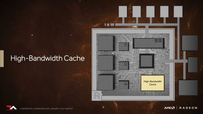
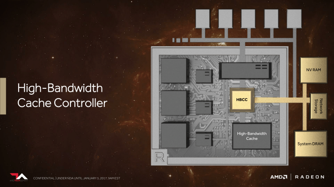
Meanwhile it’s very interesting to note that with Vega, AMD is calling their on-package HBM stacks “high-bandwidth cache” rather than “VRAM” or similar terms as was the case with Fiji products.
This is a term that can easily be misread – and it’s the one area where perhaps it’s too much of a tease – but despite the name, there are no signals from AMD right now that it’s going to be used as a cache in the pure, traditional sense. Rather, because AMD has already announced that they’re looking into other ideas such as on-card NAND storage (the Radeon Pro SSG), they are looking at memory more broadly.
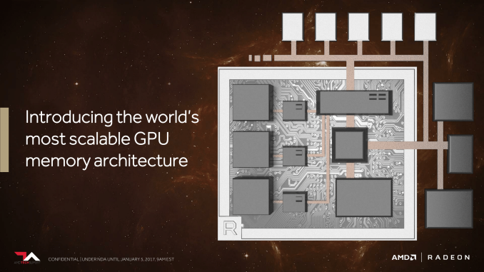
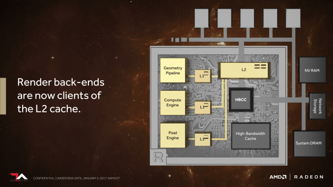
And this brings us to what AMD is calling “The World’s Most Scalable GPU Memory Architecture”. Along with supporting HBM, AMD has undertaken a lot of under-the-hood work to better support large dataset management between the high bandwidth cache (HBM2), on-card NAND, and even farther out sources like system RAM and network storage.
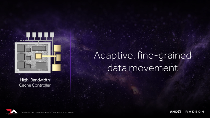
The basic idea here is that, especially in the professional space, data set size is vastly larger than local storage. So there needs to be a sensible system in place to move that data across various tiers of storage. This may sound like a simple concept, but in fact GPUs do a pretty bad job altogether of handling situations in which a memory request has to go off-package. AMD wants to do a better job here, both in deciding what data needs to actually be on-package, but also in breaking up those requests so that “data management” isn’t just moving around a few very large chunks of data. The latter makes for an especially interesting point, as it could potentially lead to a far more CPU-like process for managing memory, with a focus on pages instead of datasets.
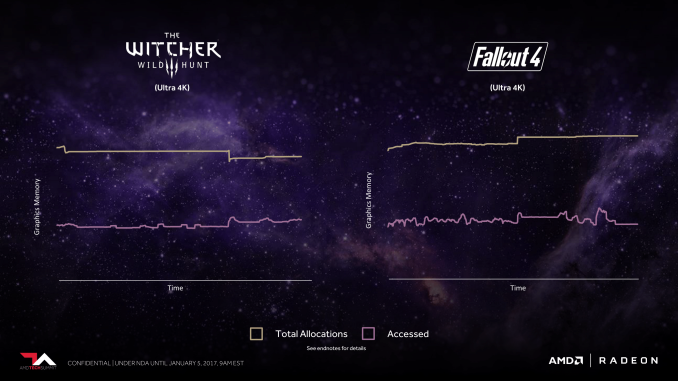
Interestingly, to drive this point home, AMD actually turned to games rather than professional applications. Plotting out the memory allocation and usage patterns of The Witcher III and Fallout 4, AMD finds that both games allocate far more memory than they actually use, by nearly a factor of 2x. Part of this is undoubtedly due to the memory management model of the DirectX 11 API used by both games, but a large factor is also simply due to the fact that this is traditionally what games have always done. Memory stalls are expensive and games tend to be monolithic use cases, so why not allocate everything you can, just to be sure you don’t run out?
The end result here is that AMD is painting a very different picture for how they want to handle memory allocations and caching on Vega and beyond. In the short term it’s professional workloads that stand to gain the most, but in the long run this is something that could impact games as well. And not to be ignored is virtualization; AMD’s foray into GPU virtualization is still into its early days, but this likely will have a big impact on virtualization as well. In fact I imagine it’s a big reason why AMD is giving Vega the ability to support a relatively absurd 512TB of virtual address space, many times the size of local VRAM. Multi-user time-sharing workloads are a prime example of where large address spaces can be useful.
ROPs & Rasterizers: Binning for the Win(ning)
We’ll suitably round-out our overview of AMD’s Vega teaser with a look at the front and back-ends of the GPU architecture. While AMD has clearly put quite a bit of effort into the shader core, shader engines, and memory, they have not ignored the rasterizers at the front-end or the ROPs at the back-end. In fact this could be one of the most important changes to the architecture from an efficiency standpoint.
Back in August, our pal David Kanter discovered one of the important ingredients of the secret sauce that is NVIDIA’s efficiency optimizations. As it turns out, NVIDIA has been doing tile based rasterization and binning since Maxwell, and that this was likely one of the big reasons Maxwell’s efficiency increased by so much. Though NVIDIA still refuses to comment on the matter, from what we can ascertain, breaking up a scene into tiles has allowed NVIDIA to keep a lot more traffic on-chip, which saves memory bandwidth, but also cuts down on very expensive accesses to VRAM.
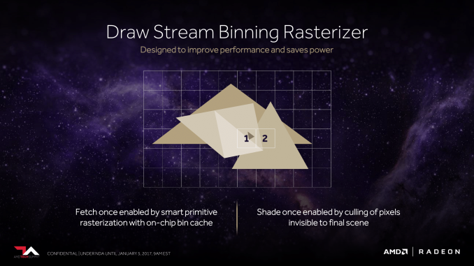
For Vega, AMD will be doing something similar. The architecture will add support for what AMD calls the Draw Stream Binning Rasterizer, which true to its name, will give Vega the ability to bin polygons by tile. By doing so, AMD will cut down on the amount of memory accesses by working with smaller tiles that can stay-on chip. This will also allow AMD to do a better job of culling hidden pixels, keeping them from making it to the pixel shaders and consuming resources there.
As we have almost no detail on how AMD or NVIDIA are doing tiling and binning, it’s impossible to say with any degree of certainty just how close their implementations are, so I’ll refrain from any speculation on which might be better. But I’m not going to be too surprised if in the future we find out both implementations are quite similar. The important thing to take away from this right now is that AMD is following a very similar path to where we think NVIDIA captured some of their greatest efficiency gains on Maxwell, and that in turn bodes well for Vega.
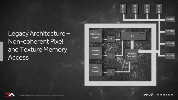
Meanwhile, on the ROP side of matters, besides baking in the necessary support for the aforementioned binning technology, AMD is also making one other change to cut down on the amount of data that has to go off-chip to VRAM. AMD has significantly reworked how the ROPs (or as they like to call them, the Render Back-Ends) interact with their L2 cache. Starting with Vega, the ROPs are now clients of the L2 cache rather than the memory controller, allowing them to better and more directly use the relatively spacious L2 cache.
This is especially significant for a specific graphics task, which is rendering to a texture (as opposed to a frame buffer to be immediately displayed). Render to texture is an especially common operation for deferred shading, and while deferred shading itself isn’t new, its usage is increasing. With this change to Vega, the ROPs can now send a scene rendered to a texture to the L2 cache, which can in turn be fetched by the texture units for reuse in the next stage of the rendering process. Any potential performance improvements from this change are going to be especially game-specific since not every game uses deferred shading, but it’s one of those corner cases that is important for AMD to address in order to ensure more consistent performance.




155 Comments
View All Comments
FireSnake - Thursday, January 5, 2017 - link
ve.ga is not accessible .... no Ryzen servers yet, haha :)Michael Bay - Thursday, January 5, 2017 - link
Desktop graphics game is lost. AMD should just close all non-gpu divisions and outright reorient towards producing specific ASIC solutions for miners, this newfangled machine bullshit and such.DATS WHERE DEM MONES BE BRAH
rpmrg - Thursday, January 5, 2017 - link
Here's another armchair analyst.Michael Bay - Thursday, January 5, 2017 - link
At least try to hide your envy next time, honey.lobz - Thursday, January 5, 2017 - link
yeah rpmrg dude, don't you ever be envious of his armchair...ddriver - Thursday, January 5, 2017 - link
People are confusing "armchair analyst" with "idiot" :)While it is disappoint for me, as I am predominantly interested in compute, vega has the makings of a good gaming GPU, disappointing for me as this comes from sacrificing high-precision performance for the sake of efficiency and optimizing for low-prevision performance, which is the precision which game graphics utilize.
extide - Thursday, January 5, 2017 - link
Well, the only bit about DP FP on the slides mentioned that it was 'configurable' -- so we don't know what we will see 1/2, 1/3, 1/4... ? Rate vs SP DP? AMD has always been more gratuitous with not disabling that higher end compute on consumer parts -- but we wont know what's actually in the silicon until later. I wouldn't be surprised to see at least one 1/2 rate DP FP part ship at some point, whether it be sold as a consumer card or only as a pro card, only time will tell.eachus - Saturday, January 14, 2017 - link
AMD has stated that Vega 20 (due in 2H18) will have 1/2 DPFP, while Vega 10 will be 1/16th. The configurable means that different chips can have different double precision rates. There is at least one additional Vega chip in the works (Vega 11) plus Navi. However, I think that 1/2 is as fast as we will see. ;-)Michael Bay - Friday, January 6, 2017 - link
But not in your case. ^_^Alexvrb - Friday, January 6, 2017 - link
Why not, his armchair is the brains of the operation! Seriously, he's totes right though... they should just throw away GPU revenue. Take chips that could otherwise be sold in several product categories, and only sell them as "newfangled machine bullshit" chips. Plus some low-margin ephemeral ASICs for miners. See, it's brilliant. Cuts down volume which saves on shipping costs. Plus it means less wafers so you don't get those pesky economies of scale benefits. Nvidia would obviously go this route too but they just don't have the balls to stop selling graphics cards. Excelsior!!