Chipworks
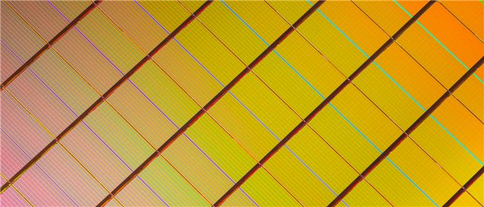
Now that the Intel Optane Memory M.2 SSDs are readily available on the open market, anyone with an electron microscope and the skills to use it can begin to probe the secrets of 3D XPoint memory that Intel and Micron have been keeping tightly under wraps since announcing the new technology in August 2015. The reverse engineering experts at TechInsights have been doing just that, and they recently published their initial findings. With some of the first high-resolution die photographs of 3D XPoint, TechInsights has provided precise measurements of the die size and memory density. The 128Gb 3D XPoint die is 206.5 mm2, much larger than is typical for modern NAND flash or DRAM but comparable to Intel's 128Gb 20nm planar MLC NAND. A large...
Early iPhone 7 Teardowns: Intel & Qualcomm Modems, TSMC SoC, 2 to 3 GB of RAM
Today is launch date for Apple’s new iPhone 7 models, and as is tradition every year, the teardowns have already begun. Both the Chipworks/TechInsights team and iFixit have completed...
97 by Ryan Smith on 9/16/2016


