Hot Chips 31 Live Blogs: Intel 10nm Spring Hill NNP-I Inference Chip
by Dr. Ian Cutress on August 20, 2019 2:55 PM EST
03:35PM EDT - .
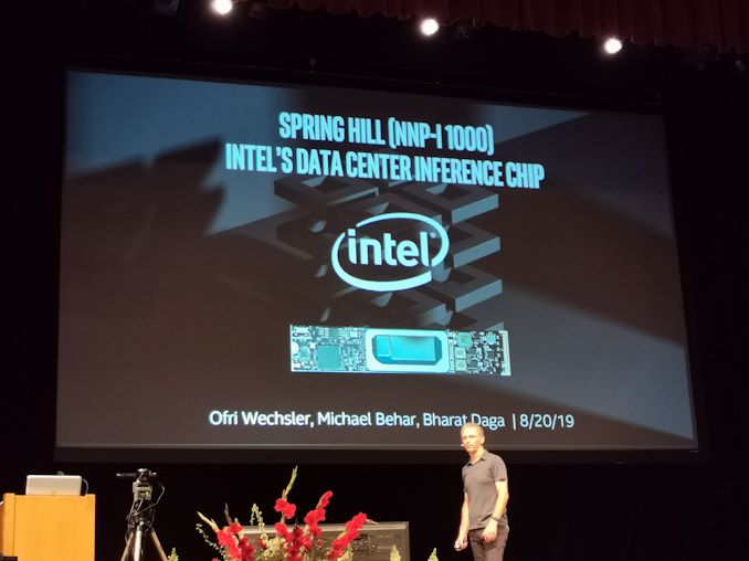
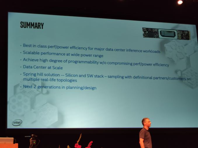
03:05PM EDT - One of Intel's future 10nm products is the Spring Hill NNP-I 1000 Inference Engine. Today the company is lifting the lid on some of the architecture behind the chip.
03:05PM EDT - This is a 10nm chip !
03:05PM EDT - More info coming. I've been briefed on this
03:06PM EDT - Haven't had time to write it up yet. But here's the live blog
03:07PM EDT - The importance of machine learning and inference
03:07PM EDT - chip architecture becomes important
03:09PM EDT - Purely internal Intel chip
03:09PM EDT - Comes in M.2 form factor and a custom form factor
03:10PM EDT - M.2 module shown comes with 16 GB DRAM onboard
03:10PM EDT - 5 minutes in and still on the intro slide
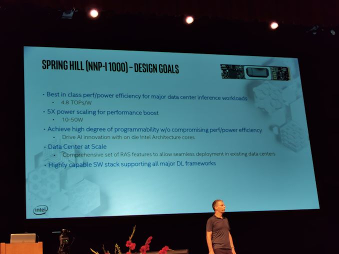
03:11PM EDT - Up to 4.8 TOPs/W
03:11PM EDT - Same silicon can go 10W to 50W
03:11PM EDT - This is a DC chip
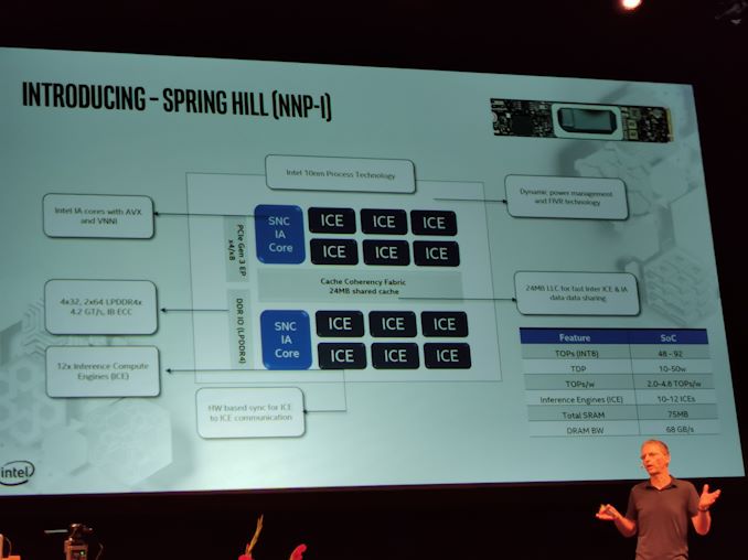
03:11PM EDT - Contains Intel Sunny Cove cores
03:11PM EDT - Highly capable SW stack supporting all major DL frameworks
03:11PM EDT - Having Sunny Cove means AVX-512 onboard
03:14PM EDT - RAS features for DC
03:15PM EDT - Still on this slide
03:16PM EDT - 2 Sunny Cove Cores, 12 Inference cores, 24 MB shared cache
03:16PM EDT - 'ICE'. But not ICE lake
03:16PM EDT - It's basically an 8-core Ice Lake chip with the graphics and 6 cores removed, and ICEs moved in
03:17PM EDT - Same DRAM support as Ice Lake
03:18PM EDT - Each of the Sunny Cove cores can control any of the 12 ICE cores
03:18PM EDT - PCIe 3.0 x4/x8 connection to the host CPU
03:18PM EDT - 75MB total SRAM, 68 GB/s DRAM BW
03:19PM EDT - 10+ process node
03:19PM EDT - Designed for other power constrained problems
03:19PM EDT - Power management same as Ice Like
03:19PM EDT - Lake
03:20PM EDT - Map workloads to allocated power budgets
03:20PM EDT - Standard PCIe device
03:21PM EDT - In 50W mode, it's obviously not an M.2 drive
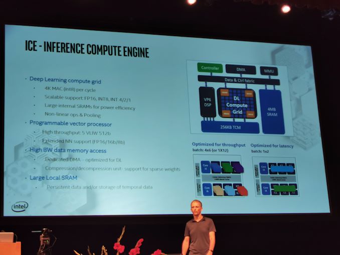
03:22PM EDT - Each ICE can do 4K MAC/cycle
03:23PM EDT - Supports FP16 / INT8/4/2/1
03:23PM EDT - Dedicated DMA optimized for DL
03:23PM EDT - Compression/decompression unit for sparse
03:24PM EDT - 4MB SRAM per ICE with 256KB TCM between Compute Grid/Vector DSP
03:24PM EDT - Tensilica V6 DSP per ICE
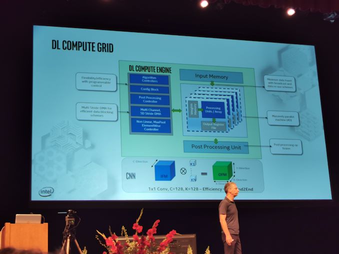
03:25PM EDT - DL Compute Engine looks like a 4D grid
03:25PM EDT - 5D Stride DMA
03:25PM EDT - Post-processing op-fusion
03:26PM EDT - Minimize data transfer
03:26PM EDT - Non Linear Maxpool ElementWise Controller
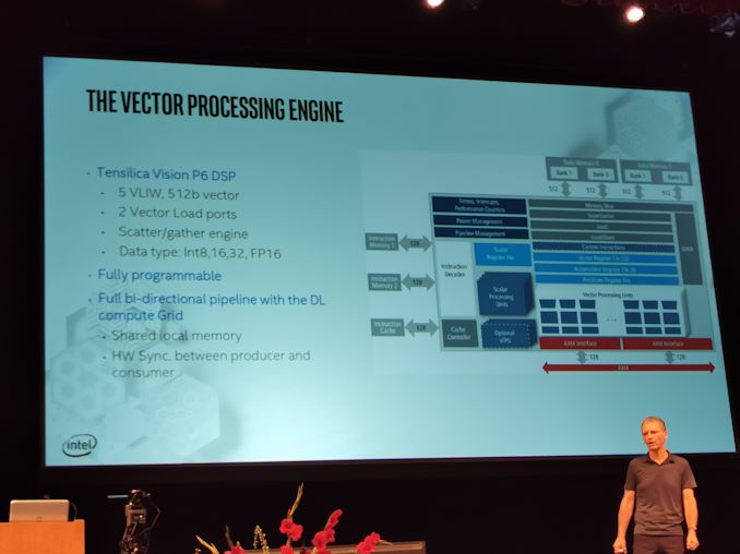
03:28PM EDT - DSP has 2 vector load ports, supports native scatter/gather engine
03:28PM EDT - Fully programmable
03:28PM EDT - bi-directional pipeline with the DL compute grid with shared local memory and hardware sync
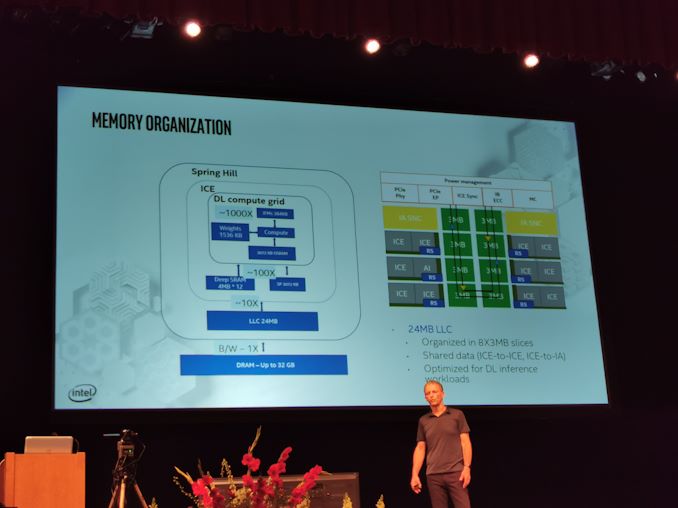
03:28PM EDT - 4 levels of memory
03:29PM EDT - It's like an 8-core Ice with the Cores ripped out with 2 ICEs put in
03:29PM EDT - Up to 32 GB of DRAM
03:29PM EDT - No BF16 support
03:30PM EDT - ResNet-50, 3600 Inferences per second at 10W
03:31PM EDT - Going form 2 to 12 cores gives 5.85x speedup
03:35PM EDT - That's a wrap. Time for lunch. Next up is TSMC Keynote at 1:45pm PT.




2 Comments
View All Comments
name99 - Sunday, August 25, 2019 - link
10W to 50W, separate chip, inference. So what's the target market? Cars?For data center inference it seems too unambitious -- surely larger, more power would make more sense? What does "Purely internal Intel chip" mean? It's not actually for sale, just an experiment living in Intel data centers (which do exactly how much inference?)
For personal use, being a separate chip seems a non-starter --- you need that NPU on the same chip as the CPU and GPU. (And presumably the good ship SS Intel is slowly turning in that direction, at its usual stately pace, and some time around 2025 will announce SoCs that do this. The more interesting question is how long AMD's cycles are, and whether THEY can learn anything from what the mobile market starting doing in 2017.)
Andy Chow - Monday, August 26, 2019 - link
You don't really need the NPU to be on the same chip as the CPU or GPU. Good example is Google's Coral TPU accelerator, which runs on a USB cable. At least this is PCIe.