NVIDIA's GeForce GT 430: The Next HTPC King?
by Ryan Smith & Ganesh T S on October 11, 2010 9:00 AM ESTIt’s been 7 months since the launch of the first Fermi cards, and at long last we’re here: we’ve reached the end of the road on the Fermi launch. Today NVIDIA is launching the final GPU in the first-generation Fermi stack into the add-in card market, launching the GeForce GT 430 and the GF108 GPU that powers it. After months of launches and quite a bit of anticipation we have the complete picture of Fermi, from the massive GTX 480 to today’s tiny GT 430.
For the GT 430, NVIDIA is taking an interesting position. AMD and NVIDIA like to talk up their cheaper cards’ capabilities in HTPC environments but this is normally in the guise of an added feature. Rarely do we see a card launched on one or two features and today is one of those launches. NVIDIA believes that they’ve made the ultimate HTPC card, and that’s the line they’re going to be using to sell it; gamers need not apply. So just what is NVIDIA up to, and do they really have the new king of the HTPC cards? Let’s find out.
| GTX 480 | GTX 460 768MB | GTS 450 | GT 430 | GT 240 (DDR3) | |
| Stream Processors | 480 | 336 | 192 | 96 | 96 |
| Texture Address / Filtering | 60/60 | 56/56 | 32/32 | 16/16 | 16/16 |
| ROPs | 48 | 24 | 16 | 4 | 8 |
| Core Clock | 700MHz | 675MHz | 783MHz | 700MHz | 550MHz |
| Shader Clock | 1401MHz | 1350MHz | 1566MHz | 1400MHz | 1340MHz |
| Memory Clock | 924MHz (3696MHz data rate) GDDR5 | 900MHz (3.6GHz data rate) GDDR5 | 902MHz (3.608GHz data rate) GDDR5 | 900MHz (1800MHz data rate) DDR3 | 790MHz (1580MHz data rate) DDR3 |
| Memory Bus Width | 384-bit | 192-bit | 128-bit | 128-bit | 128-bit |
| Frame Buffer | 1.5GB | 768MB | 1GB | 1GB | 1GB |
| FP64 | 1/8 FP32 | 1/12 FP32 | 1/12 FP32 | 1/12 FP32 | N/A |
| Transistor Count | 3B | 1.95B | 1.17B | 585M | 727M |
| Manufacturing Process | TSMC 40nm | TSMC 40nm | TSMC 40nm | TSMC 40nm | TSMC 40nm |
| Price Point | $449 | $169 | $129 | $79 | $75 |
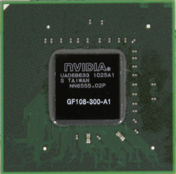
The GT 430 is based on NVIDIA’s GF108 GPU, which like the GT21x GPUs before it, is coming to retail cards last rather than first. It’s already shipping in notebooks and prebuilt HTPCs, but this is the first time we’ve had a chance to look at just the complete card. And it really is a complete card – unlike all of NVIDIA’s other desktop launches which had GPUs with disabled functional units, the GT 430 uses a fully enabled GF108 GPU. For once with Fermi, we’ll be able to look at the complete capabilities of the GPU.
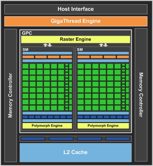
On the shader side of things, NVIDIA has taken GF106 and nearly cut it in half. We still have 1 GPC, but now it houses 2 SMs instead of 4. Each SM still contains 48 shaders, 8 texture units, and has FP64 capabilities, fulfilling NVIDIA’s commitment to FP64 capabilities (no matter how slow) on all Fermi GPUs. So yes Virginia, you can write and debug FP64 CUDA code on GF108. Attached to the shader block is 2 64bit memory controllers providing a 128bit memory bus, along with 128KB of L2 cache and a block of 4 ROPs.

For the memory NVIDIA is using DDR3, which is still common for cards under $100 given the price premium of GDDR5. Much like the GT 240 we believe this puts the GT 430 at a memory bandwidth disadvantage, and NVIDIA is already talking about working with partners on a GDDR5 version of the card in the future. We suspect that such a card will appear once 2Gbit GDDR5 is available in sufficient volume, as NVIDIA and their partners would seem to be fixated on having 1GB of RAM for now. In practice we usually find that 512MB of GDDR5 is better than 1GB of DDR3 in most cases.
Based on what we originally saw with GF104, we had expected GF108 to be a near-perfect quarter of the GF104 die: one-quarter the shaders, one-quarter the memory controllers, one quarter the ROPs. Even though GF108 has been available for some time now in mobile, OEM, and professional parts, we’ve never really taken a look at it beyond the fact that it had 96 shaders. If we had, we would have noticed something very important much sooner: it only has 4 ROPs.
For GF100-GF106, NVIDIA paired a block of 8 ROPS with a single 64bit memory controller. At the top this gave GF100 a 384bit memory bus, and down at GF106 it had a 192bit memory bus (with the GTS 450 shipping with 2 of those 3 64bit controllers active for a 128bit bus). For GF108 NVIDIA went with 2 64bit controllers to make a 128bit memory bus, which itself is not surprising since 64bit buses have extremely limited bandwidth, and that’s only suitable for bottom-tier ultra-cheap parts of which GF108 is not. So imagine our surprise when we were looking at the final spec sheet for GF108 and noticed that it didn’t have the 16 ROPs that logic dictates would be paired with a 128bit memory bus. And imagine our further surprise when that wasn’t even 8 ROPs, which is the size of a single block of ROPs or what GT214/GT216 had.
Instead NVIDIA’s thrown us another curveball here (they keep doing that) and gone with a new ROP configuration we haven’t seen before. For GF108 there are 4 ROPs in a single block, and that block is attached to the two 64bit memory controllers that make up the GPU’s 128bit memory bus. This is a surprising change since it would have required additional work on their part to make the necessary changes to their ROPs – sticking to the standard ratio would have been much easier. In any case it’s a notable change that makes GF108 something very different than we were initially expecting.

It’s the story of 4 ROPs that also sets up the positioning of the GT 430, the only retail card being released based on GF108 at the moment. With GT 430, NVIDIA has basically surrendered to AMD on performance. In a very unusual manner, you won’t find NVIDIA extoling the virtues of the card’s performance over AMD’s lineup. Even in our press briefing there was little said about gaming performance beyond the fact that it’s faster than the GT 220 and that NVIDIA believes it’s a meaningful upgrade over Intel’s IGP products due to their greater compatibility with games. Instead NVIDIA is largely selling this card upon its virtues as an HTPC card, or as NVIDIA likes to call the broader market segment: Digital Media PCs.
NVIDIA’s ace in the hole is that they have 1 thing right now that AMD doesn’t: a complete 3D stereoscopy strategy. On the hardware side this is due to the fact that GF104/106/108 all have support for HDMI 1.4a, which is necessary for full resolution 3D television/Blu-Ray and is an advantage afforded to them by the fact that AMD’s products are too old to incorporate support for HDMI 1.4a. On the other side NVIDIA has a coherent 3D strategy, with 3D Vision hardware for PC monitors, and thanks to the HDMI support for sending Blu-Ray 3D to TVs (and later this year, 3D gaming through 3D TV Play). And of course NVIDIA has bitstreaming audio capabilities for compressed lossless audio formats, bringing them up to par with AMD's audio offerings and a step up over the GT 200 series which could only support LPCM.
The long and the short of matters is that for gaming performance NVIDIA is already beat; as we’ll see even a Radeon HD 5570 DDR3 can confidently beat the GT 430, never mind the Radeon HD 5670 which can currently be found for even cheaper than the GT 430 once you factor in rebates. Even the GT 240, a card we panned hard last year is faster for the same price. With the hardware design NVIDIA has gone for, for the enthusiasts that are reading this article the GT 430 lives and dies by its HTPC capabilities; that’s NVIDIA’s position.
Moving on, since we’re looking at a low-end 40nm DirectX 11 part, this is a good time to talk about the “DX11 tax” – the fact that adding DX11 support to hardware takes up die space. We’ve already seen AMD go through this process with the 5000 series, where AMD had to spend most of their gains from the 40nm die shrink on transistors for DX11 features as opposed to transistors for overall performance. This is why cards like the Radeon HD 5450 end up being at best only as fast as the 4000 series cards they replace, and why the only major performance gains we saw when jumping generations were with GPUs that grew larger in size such as RV870. NVIDIA has to pay the same tax, and unlike AMD it’s even more obvious thanks to the fact that NVIDIA’s last-gen sub-$100 products were already 40nm.

At 585 million transistors, GF108 has outright half as many transistors as GF106, and compared to the GT21x series it has 100mil more transistors than GT216 (card: GT 220) and about 150mil fewer than GT 214 (card: GT 240). Lest we forget that Fermi was a major architecture revision for NVIDIA, they still had to pay the DX11 tax – if they were to add DX11 functionality to the GT21x series, all of their products would get larger and less profitable. How they chose to pay this tax was why we’re talking about GF108 only having 4 ROPs.
On the diagrams we use to showcase GPU architectures ROPs are drawn fairly small, but in reality they’re disproportionally drawn to make it easier to fit everything else in. Modern ROPs are actually pretty big, especially 16 of them as NVIDIA’s normal ratios would call for. They aren’t a massive fraction of the GPU, but they’re big enough that they can’t hide from GPU designers looking for ways to make an economical GPU. NVIDIA needs shader cores for gaming and compute alike, they need memory controllers and cache to feed those shaders, and they need fixed function units to glue the GPU together. ROPs are necessary as arbitrators to the memory controllers and for graphics rendering, but ultimately they’re one of the few graphics-only functional units next to the texture units.
And thus NVIDIA chose to pay the DX11 tax by cutting down on ROPs. This redesign no doubt added some extra work for them, but the end result was that it allowed them to get GF108 down to the die size and power consumption of the product we see today. NVIDIA’s rational for choosing the ROPs comes down to the belief that they’re one of the least important parts of a GPU for a value product, as features such as anti-aliasing are not usually used with these products, and as we’ve seen even additional ROPs won’t make these cards playable at higher resolutions such as 1680x1050. As a result the ROPs got the axe so that NVIDIA could bring a small die GPU with DX11, low power consumption, and better than GMA/5450 performance to market.
Funny enough NVIDIA won’t give us the actual size of GF108 (they haven’t done this for any Fermi parts), but using a ruler we’d estimate the size to be 11mm x 10.5mm, or roughly 116mm2. As with transistor count this puts it between GT214 and GT216 (being closer to GT216), or roughly the same size as AMD’s Redwood GPU in the 5500/5600 families. The card’s TDP is rated at 49W, which should actually be lower than the GT216-based GT 220, even though GT216 was a smaller GPU using fewer transistors.
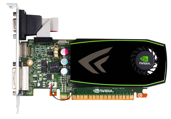
As for today’s launch, as is common with low-end products NVIDIA is leaving the launch in the hands of its partners. NVIDIA did produce a reference design for internal use, but it’s not being used by any shipping cards, nor were reviewers given the reference design. Instead all the cards you’ll see today, including the Asus card we’re reviewing today, are vendor custom cards.
We’ve attached a small gallery of card designs that will be shipping. There’s a complete range of cards, including full and half-height cards, and of course the obligatory passively cooled cards. There’s even a half-height passive card from Sparkle listed if you have that specific itch to scratch.
NVIDIA put the MSRP at $80, and while there aren’t any reference designs to tie this to we expect the first wave of cards to stick to this price point. At $80 the GT 430 goes directly up against the Radeon HD 5570 (DDR3 & GDDR5), sale-priced Radeon 5670s, the GT 240, and even the venerable 9800GT. All of these cards are faster in gaming performance, which is why NVIDIA’s strengths need to lie in HTPC performance and overall power consumption.
| October 2010 Video Card MSRPs | ||
| NVIDIA | Price | AMD |
| $700 | Radeon HD 5970 | |
| $500 | ||
|
|
$360 | Radeon HD 5870 |
| $300 | ||
|
|
$270 | Radeon HD 5850 |
| $230 | ||
| $220 | ||
| $170 | Radeon HD 5830 | |
| $130 | Radeon HD 5770 | |
|
GeForce GT 430
|
$80 | Radeon HD 5670/5570 |


120 Comments
View All Comments
n9ntje - Monday, October 11, 2010 - link
Sad to see Nvidia doesn't live up to expectations, while they want us to believe that they have a perfect HTPC card, it isn't.To most people, image quality counts. 3D is still a niche.
IceDread - Monday, October 11, 2010 - link
Yeap, it's always best if the competition is even, gives us the best prices.medi01 - Monday, October 11, 2010 - link
I am afraid market is too slow to react to nVidia having worse products, AMD has nowhere near market share that it deserves to have.We can't expect one player to dominate all the time. So when the underdog creates superior products, it should benefit from it. But this is not the case in GPU market, unfortunatelly, as nVidia still keeps much bigger market share, than AMD.
dnd728 - Monday, October 11, 2010 - link
I've tried quite a few ATI/AMD cards over the years, including the latest 5000 series, and to date not a single one of them worked right, i.e. without keep crashing Windows.It could be one reason.
electroju - Monday, October 11, 2010 - link
I agree and I have also used ATI and AMD graphics over the years. AMD graphics writes the worst software or drivers from a reputable company. I go with nVidia because I care for reliability and stability. I do not mind spending money on nVidia graphics because the money goes towards software development. The cost of AMD graphics is too low to provide enough for software development.Zoomer - Monday, October 11, 2010 - link
I have personally found nvidia cards to have inferior hardware quality. This was very evident from the time when quality dacs for vga mattered, and nvidia cards absolutely sucked at that. Further suboptimal decisions made their cards meh.Software wise, I thought nvidia's software quality peaked around the time of the detonators.
AmdInside - Monday, October 11, 2010 - link
DACs depended on the maker of the card. Quadro NVS cards which were made by NVIDIA were regarding as having excellent 2D image quality over analog display. Sadly a lot of NVIDIA partners used cheap DACs on some of their cards.mentatstrategy - Wednesday, October 13, 2010 - link
Nvidia Fanboi: I have used ati cards and they suck!ATI Fanboi: I have used nvidia cards and they suck!
heflys - Monday, October 11, 2010 - link
Hmmm....Haven't had a problem with ATi/AMD drivers thus far.duploxxx - Friday, October 15, 2010 - link
perhaps you need to read a bit more and see how many 1000's have been recently been affected by this awesome nvidia reliability and stability when they all had to throw away there graphic cards and laptops.