NVIDIA Updates GPU Roadmap; Announces Volta Family For Beyond 2014
by Ryan Smith on March 19, 2013 7:15 PM EST
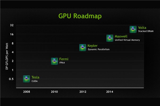
As we covered briefly in our live blog of this morning’s keynote, NVIDIA has publically updated their roadmap with the announcement of the GPU family that will follow 2014’s Maxwell family. That new family is Volta, named after Alessandro Volta, the physicist credited with the invention of the battery.
At this point we know very little about Volta other than a name and one of its marque features, but with how NVIDIA operates that’s consistent with how they’ve done things before. NVIDIA has for the last couple of years operated on an N+2 schedule for their public GPU roadmap, so with the launch of Kepler behind them we had been expecting a formal announcement of what was to follow Maxwell.
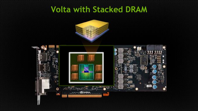
In any case, Volta’s marque feature will be stacked DRAM, which sees DRAM placed very close to the GPU by placing it on the same package, and connected to the GPU using through-silicon vias (TSVs). Having high bandwidth, on-package RAM is not new technology, but it is still relatively exotic. In the GPU world the most notable shipping product using it would be the PS Vita, which has 128MB of RAM in a wide-IO (but not TSV) manner. Meanwhile NVIDIA competitor Intel will be using a form of embedded DRAM for their highest-performance GT3e iGPU for their forthcoming Haswell generation CPUs.
The advantage of stacked DRAM for a GPU is that its locality brings with it both bandwidth and latency benefits. In terms of bandwidth the memory bus can be both faster and wider than an external memory bus, depending on how it’s configured. Specifically the close location of the DRAM to the GPU makes it practical to run a wide bus, while the short traces can allow for higher clockspeeds. Meanwhile the proximity of the two devices means that latency should be a bit lower – a lot of the latency is in the RAM fetching the required cells, but at the clockspeeds GDDR5 already operates at the memory buses on a GPU are relatively long, so there are some savings to be gained.
NVIDIA is targeting a 1TB/sec bandwidth rate for Volta, which to put things in perspective is over 3x what GeForce GTX Titan currently achieves with its 384bit, 6Gbps/pin memory bus (288GB/sec). This would imply that Volta is shooting for something along the lines of a 1024bit bus operating at 8Gbps/pin, or possibly an even larger 2048bit bus operating at 4Gbps/pin. Volta s still years off, but this at least gives us an idea of what NVIDIA needs to achieve to hit their 1TB/sec target.
What will be interesting to see is how NVIDIA handles the capacity issues brought on by on-chip RAM. It’s no secret that DRAM is rather big, and especially so for GDDR. Moving all of that RAM on-chip seems unlikely, especially when consumer video cards are already pushing 6GB (Titan). For high-end GPUs this may mean NVIDIA is looking at a split RAM configuration, with the on-chip RAM acting as a cache or small pool of shared memory, while a much larger pool of slower memory is attached via an external bus.
At this point Volta does not have a date attached to it, which is unlike Maxwell which originally had a 2013 date attached to it when first named. That date of course slipped to 2014, and while it’s never been made clear why, the fact that Kepler slipped from 2011 to 2012 is a reminder that NVIDIA is still tied to TSMC’s production schedule due to their preference to launch new architectures on new nodes. Volta in turn will have some desired node attached to its development, but we don’t know what at this time.
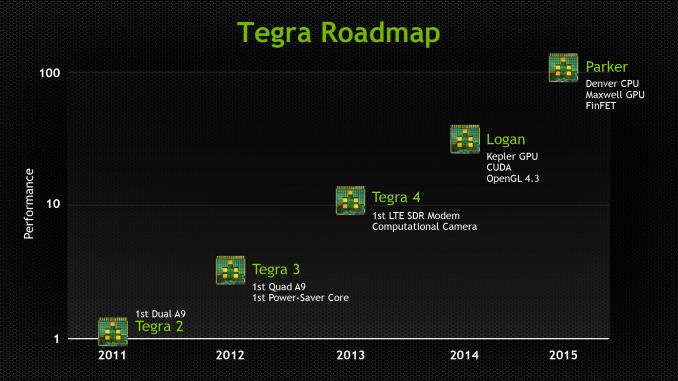
With TSMC shaking up its schedule in an attempt to catch up to Intel on both nodes and technology, the lack of a date ultimately is not surprising since it’s difficult at best to predict when the appropriate node will be ready 3 years out. On that note it’s interesting to note that while NVIDIA has specifically mentioned FinFET transistors will be used on their Parker SoC, they have not mentioned FinFET for Volta. Coming from their investor meeting the question came up, and while it wasn’t specifically denied we were also left with no reason to expect Volta to be using FinFET, so make of that what you will.
Meanwhile, in NVIDIA tradition they’ve also thrown out a very rough estimate of Volta’s performance by plotting their GPUs against a chart of FP64 performance per watt. Today Kepler is already at roughly 5.5 GFLOPS/watt for K20X, while Volta is plotted at 24ish. Like the rest of the GPU industry NVIDIA remains to be power constrained, so at equal TDPs we’d expect roughly four times the performance of K20X, which would put total FP64 performance at around 5 TFLOPS. But again, all of this is early into a GPU that will not be released for years.
Finally, while Volta is capturing the majority of the press due to the fact that it’s the newest GPU coming out of NVIDIA, this latest roadmap does also offer a bit more on Maxwell. Maxwell’s marque feature as it turns out is unified virtual memory. CUDA already has a unified virtual address space available, so this would seemingly go beyond that. In practice such a technology is important for devices integrating a GPU and a CPU onto the same package, which is what the AMD-led Heterogeneous System Architecture seeks to exploit. For NVIDIA their Parker SoC will be based on Maxwell for the GPU and Denver for the CPU, so this looks to be a feature specifically setup for Parker and Parker-like products, where NVIDIA can offer their own CPU integrated with a Maxwell GPU.


17 Comments
View All Comments
jjj - Tuesday, March 19, 2013 - link
Pretty sure you messed up on Volta.The DRAM is stacked and it uses TSV, so you got DRAM over DRAM and they should be able to put quite a bit around the GPU ( they might as well use Micron's Hybrid Memory Cube since that's advertised at 1TB too but that one is a bit different having the logic layer at the base).
The GPU should be connected to the RAM through the silicon substrate , don't think they ever said "silicon interposer" but i imagine that's what they are doing.
Wish they would use it in mobile for NAND and RAM, maybe we they go there when the industry goes with RRAM , shouldn't be that far , we should get 3D NAND in 2015-2016 and RRAM not too long after.
MrSpadge - Wednesday, March 20, 2013 - link
You're right: from nVidias picture it looks like the die-stacked DRAM will be placed on-package. This solves the capacity issue directly :)Stacking GPU and DRAM would create serious cooling problems: the heat would have to flow through all DRAM dies before it could reach the cooler, in return the chip would run much hotter for a given cooler. I guess that's why Intel reserves the tier 3 GPU with embedded DRAM for mobile Haswell, where there's not as much heat to get rid off.
warezme - Monday, April 1, 2013 - link
If you 3D stack your die with DRAM on one side and the core on the other side (visualize a chip design that has an opening on the die to both the front and back of the card motherboard). You could the cool both the DRAM side and the GPU side independently and even with the same cooler if you offset the board to center on your slot better. It would be a new design but not that exotic really.Kevin G - Tuesday, March 19, 2013 - link
The question for Maxwell is what architecture is its virtual memory schema tuned? The obvious answer for the desktop is x86 but if nVida wants to scale this technology into the mobile arena they'll also have to support ARM's memory management.The other thing worth pondering in that context is how closely tied Project Denver is to Maxwell.
spigzone - Tuesday, March 19, 2013 - link
So when Nvidia finally releases it's first HSA style architecture, AMD will be releasing it's 3rd generation, massively supported, HSA APUs?TheJian - Wednesday, March 20, 2013 - link
Considering they're losing 1.18 Billion last year and on track to produce another loss this year I'm not sure what your point is? NV made 725mil during the same time and added ~300mil to their cash, while buying back $100mil in stock AND paying a dividend. Until AMD makes money or tops the supercomputer list (where NV dominates now with Titan) it would appear bragging rights over who beat who to HSA means nothing correct? It wouldn't matter if AMD was on their 10th gen if they still can't top their competition with it. NV hired ~800 people over the last ~2years. AMD laid off 30% of their workforce. How does that help you vault to #1 in the future? What's worse? No ARM soc from AMD until next year and probably late next year for any revenue. But even worse, NV will be on Rev5 of socs by then which as with T4 will have a modem (and T5 will surely include cdma etc thus serving everyone, where T4 is limited). Being in the SOC race NOW is more important than the HSA race or all the numbers would be in AMD's favor right?http://arstechnica.com/gadgets/2013/03/nvidias-nex...
Then again, their HSA isn't really due to be used until 2014 when memory is fully shared & a unified address space (kaveri) :) Currently copying the data twice/to and from cpu/gpu makes HSA useless. They will get nothing from this until 2014 at the earliest. Sometimes, being 1st isn't really being ahead at all ;) We still have die shrinks working also, which slows this progression to HSA type stuff (we haven't hit the nm wall yet), and you need software to take advantage of all this anyway (that's a few years off).
If consoles don't pay off in a big way AMD will go further into debt as their recent 164mil renting of their Austin land won't do squat vs. another Billion loss this year. I expect consoles to suck this time (dev support dropping already for Vita, wiiu/3ds sucking wind shows this already), and when sales at xmas suck they'll just cancel projects and head further to mobile. They need to quit giving away top games which directly steals from their gpu profits when a card sells. Not to mention the IDEA that if you have to give that much crap away to sell your cards you must suck (no matter what the perf REALLY is of your cards - it looks desperate to a lot of people or they'd own more market share right?) vs. the competition who practically gives nothing (free to play crap? costing them next to nothing also). Market share of discrete gpu's shows this as NV controls ~65% of it and has for years (up from 53% in 2011).
AMD is currently funding R&D with more debt and selling or renting everything they have, while NV funds it with profits and Intel payments. The last Intel payment is 2016. So they'll be using some free money to do R&D for the next few years on top of whatever they profit (which shows no sign of slowing down, they just set records for revenue, margins and cash). The employee reduction cost is shown by how long it took AMD to get a decent driver to compete in gpus (never settle driver, pre this driver they got smacked all year as hardocp recently discussed). Another sign is the delay in Kaveri into 2014 most likely which of course allows NV to put maxwell later (both look Q1 now). They couldn't afford to R&D for consoles and discrete gpu updates at the same time (unfortunately). You can't outfox your enemy on a visa card forever if at all. No answer to Titan doesn't look good either (no matter how overpriced someone thinks it is).
Finally, AMD isn't in the top ten supercomputers (feeding the K20x in titan doesn't count, amd isn't doing the work here). NV is in TWO of them and I'm sure more to follow as others add K20x machines and tegra starts to feed the gpus for a green machine though Italy just claimed per/watt lead with K20x supposedly and piz daint just got announced:
http://blogs.nvidia.com/2013/01/just-mix-water-wit...
So again, what evidence is there that being on HSA early is working so far? Your comment insinuates NV is behind. I think it's quite the opposite based on all the data. This may have been a totally different story if AMD had taken the time/money they spent on consoles and devoted it instead to Socs and discrete gpus. Not much money will be made on 35mil units of consoles this year (if they even sell that total together) vs. a billion unit market in tablets/phones and growing every year. NV is moving ~20% of their revenue via tegra already and will grow that this year with T4/T4i. AMD spent their wad on a dying market (consoles/handhelds) and are losing badly in the two markets they have now (cpu/gpu, cpu's lost ~325mil, and gpus only made ~22mil...OUCH). They seem to keep repeating this losing formula and it doesn't look to change for FY2013.
Kevin G - Wednesday, March 20, 2013 - link
AMD's lead for HSA is going to be measured in months, not full generations of hardware. It'll be arriving in 2013 at the very least with the PS4. Dev kits are currently in the hands of developers with early prototype hardware. Kaveri and Maxwell are both 2014 parts and without further details it is difficult to determine which will arrive first. The other wild card for 2013/2014 are discrete HSA GPU's from AMD. All indications point toward AMD arriving first with a unified address space but it won't ultimately be a significant lead.As for AMD's position in the Top500, they've been there before. Tianhe-1A, the other nVidia based system referenced, used to use AMD GPU's prior to an upgrade. Though I wouldn't use the Top500 as a good metric as both nVidia's and AMD's GPGPU boards are not seen as viable options by many due to the lack of key RAS features (ECC etc.). Performance of these cards are good given an extremely parallel workload but if scientists cannot trust the integrity of the results, they're worthless.
Ktracho - Wednesday, March 20, 2013 - link
NVIDIA's Tesla boards have had ECC since at least the last generation (Fermi). That's one reason why Cray is willing to use these boards in their supercomputers.Kevin G - Thursday, March 21, 2013 - link
EDC, not traditional ECC. The memory bus width is not explicitly widened to support the extra parity bits for ECC. Conceptually nVidia's EDC is uses a technique similar to RAID5 which utilizes existing memory channels and reduces overall memory capacity by shuffles parts of the parity across all of them. This does allow for protection from common soft errors like ECC.The downside is that memory transaction involved the entire width of the memory bus where as previously each channel could operate autonomously depending on requests. nVidia tacked on EDC on Fermi with a hardware/software mix which significantly decreases memory bandwidth. EDC on GK110 and Tahiti have a bit more hardware support for EDC so bandwidth impact isn't as dire but still present.
EDC with hard errors is an interesting case for GPU's. Modern ECC implementations can work around a single DRAM chip failure on a DIMM and safely move the data to another DIMM (and a few high end servers will even allow memory hot swapping). Fermi had no means of recovering from a hard memory error due to its partial use of software. I'm unsure if GK110 and Tahiti would be able to migrate data off of the card in the advent of a hard memory failure and I'm certain that they cannot continue to operate normally.
Still GPU's have relatively weak RAS compared to traditional server hardware and it is a reason why some are currently waiting for GPU's to mature a bit further.
Winterblade - Tuesday, March 19, 2013 - link
I wonder what kind of CPU will denver be, a customized ARM A57/A53 big.LITTLE setup maybe?? Will they finally get a x86 license?? or maybe a fully new architecture??Honestly I cannot stop marvelling every time I see this kind of roadmaps, we live in great times for tech junkies :D