AMD Announces FirePro W9100
by Ryan Smith on March 26, 2014 1:00 PM EST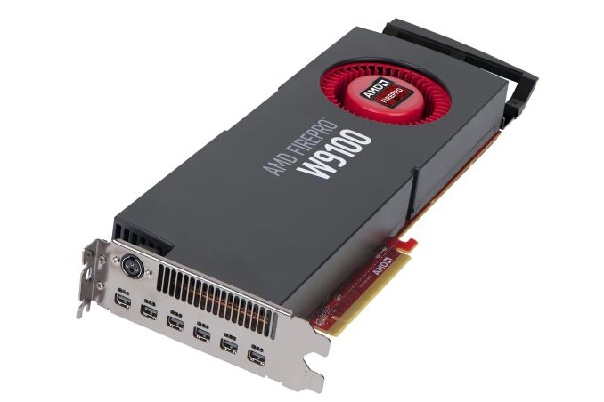
In what’s proving to be a busy week for GPU news, AMD has just wrapped up their webcast announcing their next flagship FirePro product. Dubbed the FirePro W9100, AMD’s latest card is their expected refresh of their FirePro product lineup to integrate the company’s recently launched Hawaii family of processors.
As Hawaii itself was a small but important refresh to Tahiti and the GCN architecture, the same can be said of the FirePro W9100 compared to the FirePro W9000. Other than some gaming-exclusive features such as TrueAudio, Hawaii’s biggest changes were the Asynchronous Compute Engine (ACE) additions that are part of GCN 1.1, the wider 4 primitive geometry pipeline, and of course the overall increase in performance and performance per watt compared to Tahiti. So from a technical perspective W9100 stands to be a relatively straightforward improvement to what W9000 has offered thus far.
| AMD FirePro W Series Specification Comparison | ||||||
| AMD FirePro W9100 | AMD FirePro W9000 | AMD FirePro W8000 | AMD FirePro W7000 | |||
| Stream Processors | 2816 | 2048 | 1792 | 1280 | ||
| Texture Units | 176 | 128 | 112 | 80 | ||
| ROPs | ? | 32 | 32 | 32 | ||
| Core Clock | ? | 975MHz | 900MHz | 950MHz | ||
| Memory Clock | ? | 5.5GHz GDDR5 | 5.5GHz GDDR5 | 4.8GHz GDDR5 | ||
| Memory Bus Width | ? | 384-bit | 256-bit | 256-bit | ||
| VRAM | 16GB | 6GB | 4GB | 4GB | ||
| Double Precision | 1/2? | 1/4 | 1/4 | 1/16 | ||
| Transistor Count | 6.2B | 4.31B | 4.31B | 2.8B | ||
| TDP | ? | 274W | 189W | <150W | ||
| Manufacturing Process | TSMC 28nm | TSMC 28nm | TSMC 28nm | TSMC 28nm | ||
| Architecture | GCN 1.1 | GCN 1.0 | GCN 1.0 | GCN 1.0 | ||
| Warranty | 3-Year | 3-Year | 3-Year | 3-Year | ||
| Launch Price | ? | $3999 | $1599 | $899 | ||
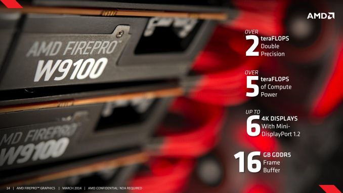
As far as specifications are concerned, it should come as no surprise that W9100 is going to look a lot like AMD’s Radeon R9 290X, their flagship consumer product. W9100 uses a fully enabled Hawaii GPU, so we’re looking at 2816 SPs spread out over 44 CUs. Unfortunately we don’t have the clockspeeds at this time, so we don’t know just how much faster W9100 is on paper versus W9000. However the increase in CUs alone is on the order of 38%, and this doesn’t take into account the improved ACEs and memory bus feeding Hawaii
Speaking of the memory bus, we don’t have the specific width or clockspeeds there either, but we know that AMD has packed W9100 with a ton of memory. 16GB of memory to be precise, which would be as much memory as Hawaii would be able to handle using current generation 8Gb GDDR5 modules. Compared to even W9000, which was relatively large for its time at 6GB, this is huge for a workstation card.
Meanwhile it’s interesting to note that while AMD hasn’t published clockspeed numbers they have published rough performance numbers for both FP32 and FP64. FP32 is rated for over 5 GFLOPS and FP64 is rated for over 2 GFLOPS. The math on that doesn’t work out conclusively – if it’s anything like NVIDIA’s GK110, then there may be additional power requirements that influence performance under FP64 mode – but these numbers point to Hawaii having 1/2 rate FP64 performance. As a reminder 290X was rated at 1/8, so this would mean Hawaii has a much higher rate than what was enabled on AMD’s consumer cards. In fact this would put Hawaii’s native FP64 rate (as a ratio of FP32 performance) as being higher than any other GPU, the next-closest GPU being NVIDIA’s GK110 at 1/3 rate FP64.
Beyond that, we don’t have any further details on the card at this time. W9100 is not launching today – we hear the launch should be soon after – so availability and pricing have not been released thus far. The best we can do is point to the W9000’s launch price of $3999 as some kind of guidance on where it may come in.
Shifting gears for a bit, while AMD was careful on releasing details ahead of the launch of the W9100, they spent some time going in depth into how the card fits into their long-term plans, and what markets they’re pursuing with the card. FirePro continues to pull double duty as AMD’s workstation graphics card and workstation compute card, centered around the capabilities of OpenCL. So AMD is looking to put together a product that can serve both markets well, especially in the case of cross-over applications that make use of both aspects of the card.
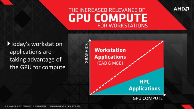
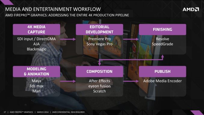
Of those aspects, AMD is definitely pushing the compute side harder this time around as opposed to the FirePro W9000 launch in 2012, as the nature of the market has changed. Traditional graphics-heavy professional applications (e.g. AutoCAD) are still as power hungry as ever – if not more so due to the rise of 4K monitors – and meanwhile the amount of compute work being generated by these programs is increasing. This goes for both programs using compute in a more straightforward way, such as running mechanical simulations, and programs leveraging compute for graphics related tasks such as video encoding and image processing. And for both of these tasks AMD is banking on their 16GB of VRAM giving them a performance advantage due to the larger working sets such a large memory configuration can hold.
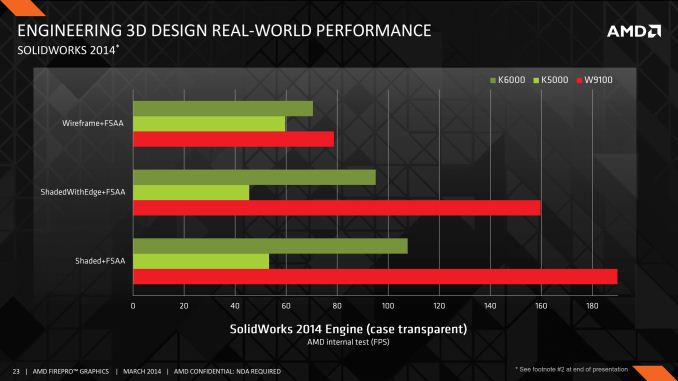
On that note, AMD has published a few benchmarks ahead of the launch of the card. But as always, these are best take with a grain of salt as they’re almost certainly best-case numbers for their hardware and software stack.
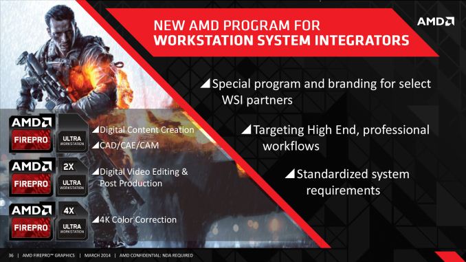
Moving on, along with the announcement of the W9100, AMD has also announced that they will be introducing a new workstation branding initiative to go with the card. Dubbed the “Ultra Workstation” initiative, the program will have 3 tiers of workstations, indicating how many GPUs they have in them and what kind of tasks AMD is recommending for them based on resource requirements and how well major applications scale to that many GPUs.
All of the Ultra Workstation tiers will have a minimum of 32GB of system memory, at least one 8 core CPU, and of course at least one W9100.
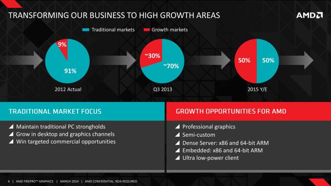
Finally, the launch of the W9100 also brings with it a brief update on AMD’s overall transformation in their product offerings, and their current market share. AMD’s share of the professional GPU market is up to 18%, which is still well off of their heyday years ago, but a solid improvement from where they were at the launch of the W9000. To that end professional graphics and compute continues to represent a major growth opportunity for the company, as the other 82% of that market share belongs to NVIDIA, and stealing even a small part of it would significantly improve AMD’s position. Next to their APU offerings – including semi-custom designs and ARM designs – the discrete GPU market for professional graphics is AMD’s final target for significant growth.
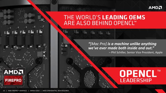
Part of that growth will in turn come from essential OEM wins. AMD’s win of the GPU contract for Apples recently launched Mac Pro is a big deal for the company, as you’d expect, as the Mac Pro is a very prestigious win. It remains to be seen just what it means for sales volumes of AMD FirePro products, but it’s a win that AMD can promote to software developers and potential customers alike.




31 Comments
View All Comments
Ian Cutress - Wednesday, March 26, 2014 - link
Time for a new card for that 6x 4K HTPC (!). Seriously though, the GDDR5 chips to make a 16GB card are not commonplace and probably made by one company. That means 16 Gbit chips to make a 512-bit bus. Sapphire just put 8 GB on the R9 290X, so here goes AMD with one better. I wonder if clock speeds have to come down because of that. Either way, 1/2 DP with the larger memory buffer are big pluses. I hope Supermicro or someone has a full Ultra Workstation that I can look at during Computex.ddriver - Wednesday, March 26, 2014 - link
Clock speed will likely not be as nigh as gaming series, but who cares, with 16 gigs of ram on board, snap 4 of those on a workstation mobo with 64 gigs of ram and you got yourself a mini supercomputer at home. Build a few, get a good 10 gbit switch and you got yourself a computer farm cluster.mczak - Wednesday, March 26, 2014 - link
You are very wrong about the gddr5 chips required not being common. Nowadays just about everyone produces (and graphic card manufacturers are using, ps4 too even) 4 gbit chips (but 2 gbit chips are still used too on some cards, most notably on 2GB 256bit cards). Since the gddr5 chips are 32bit wide, you require 16 gddr5 chips - 16 4 gbit chips give 8GB of memory. But gddr5 can use a so called clamshell mode, where you use 2 chips in a 2x16bit mode to make a 32bit wide channel. So, for a 16GB card, you simply use 32 4gbit chips in clamshell mode. (nvidia though of course due to only having a 384bit bus, is restricted to 12GB.)mczak - Wednesday, March 26, 2014 - link
That should have been "require 16 gddr5 chips for a 512bit bus".Kevin G - Wednesday, March 26, 2014 - link
Couldn't they use two 8 GBit chips on the same bus? Some previous workstation cards did so with GDDR5 to increase capacity.yasamoka - Thursday, April 3, 2014 - link
You don't have to use 8 chips for a 512-bit = 8x64-bit memory bus. The 7970 uses 12 chips for a 384-bit bus, so this could be using 16 8Gbit chips.extide - Wednesday, March 26, 2014 - link
This would be interesting, and a bit disappointing if it is true that the W9100 has 1/2 FP64 where as R9 290(x) have 1/8 FP64. Up until now, the consumer Radeon cards were never cut down and always had full performance FP64, compared to the FirePro versions. Unfortunately it seems they are probably following nVidia's lead here, and cutting the FP64 capabilities on their consumer lines, like nVidia does on Geforce vs Quadro/Tesla.coder543 - Wednesday, March 26, 2014 - link
I don't know if AMD is making Radeon cards 'cut down' in this case. It would be nice to hear the technical side of the matter, but it could be that AMD is simply binning the chips and only a small number can sustain the clock frequencies necessary to have 1/2 FP64, or that they're upgrading the chip design for the W9100 so that it can do 1/2 FP64. It's possible they're simply releasing artificially limited chips like nVidia does, but that isn't the feeling I'm getting here.**Feelings can be wrong.
SaberKOG91 - Wednesday, March 26, 2014 - link
The way I understand it, the floating point units on the consumer versions have a different pipeline width altogether. The pipeline is narrower in favor of higher FP32 throughput, but that makes the double precision take longer to process. This also allows more room for integer units if I'm not mistaken (thus the increased mining capacity of desktop parts).On the workstation grade parts, the integer side is reduced and the floating point width is increased in favor of the faster FP64 performance needed for HPC and 3D modelling work-flows. This increased floating point performance, coupled with application certifications, has always made these cards more expensive than the consumer parts with the same core count.
twoodrow - Sunday, March 30, 2014 - link
Where did you come across this information on the architecture?