AMD Announces Radeon R9 285, Shipping September 2nd
by Ryan Smith on August 23, 2014 7:00 PM EST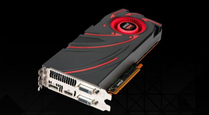
During their 30 years of graphics celebration, today AMD announced a forthcoming addition to the Radeon R9 200 graphics card lineup. Launching on September 2nd will be the company’s new midrange enthusiast card, the Radeon R9 285.
The R9 285 will take up an interesting position in AMD’s lineup, being something of a refresh of a refresh that spans all the way back to Tahiti (Radeon 7970). Spec wise it ends up being extremely close on paper to the R9 280 (née 7950B) and it’s telling that the R9 280 is no longer being advertised by AMD as a current member of their R9 lineup. However with a newer GPU under the hood the R9 285 stands to eclipse the 280 in features, and with sufficient efficiency gains we hope to see it eclipse 280 in performance too.
| AMD GPU Specification Comparison | ||||||
| AMD Radeon R9 290 | AMD Radeon R9 280X | AMD Radeon R9 285 | AMD Radeon R9 280 | |||
| Stream Processors | 2560 | 2048 | 1792 | 1792 | ||
| Texture Units | 160 | 128 | 112 | 112 | ||
| ROPs | 64 | 32 | 32 | 32 | ||
| Core Clock | 662MHz | 850MHz | ? | 827MHz | ||
| Boost Clock | 947MHz | 1000MHz | 918MHz | 933MHz | ||
| Memory Clock | 5GHz GDDR5 | 6GHz GDDR5 | 5.5GHz GDDR5 | 5GHz GDDR5 | ||
| Memory Bus Width | 512-bit | 384-bit | 256-bit | 384-bit | ||
| VRAM | 4GB | 3GB | 2GB | 3GB | ||
| FP64 | 1/8 | 1/4 | ? | 1/4 | ||
| TrueAudio | Y | N | Y | N | ||
| Typical Board Power | 250W | 250W | 190W | 250W | ||
| Manufacturing Process | TSMC 28nm | TSMC 28nm | TSMC 28nm? | TSMC 28nm | ||
| Architecture | GCN 1.1 | GCN 1.0 | GCN 1.1? | GCN 1.0 | ||
| GPU | Hawaii | Tahiti | Tonga? | Tahiti | ||
| Launch Date | 11/05/13 | 10/11/13 | 09/02/14 | 03/04/14 | ||
| Launch Price | $399 | $299 | $249 | $279 | ||
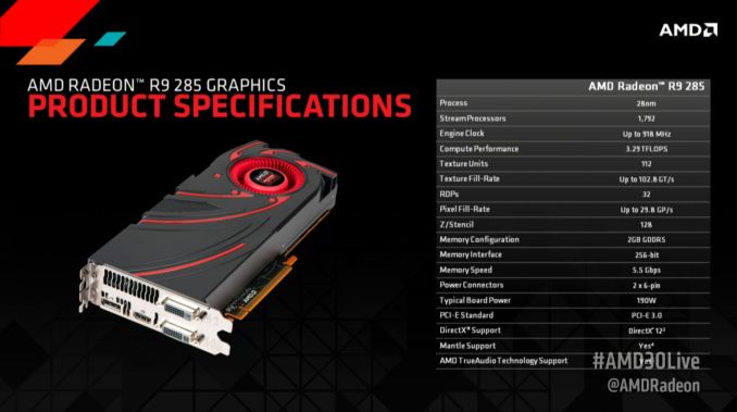
Looking at the raw specifications, the R9 285 is a 1792 stream processor Graphics Core Next product. Paired with these SPs are 112 texture units (in the standard 16:1 ratio), and on the backend of the rendering pipeline is 32 ROPs. As is unfortunately consistent for AMD, they are not disclosing the product’s base clockspeed, but they have published the boost clockspeed of 918MHz.
Meanwhile feeding R9 285’s GPU falls to the card’s 2GB of GDDR5. This is on a 256-bit bus, and is clocked at 5.5GHz for a total memory bandwidth of 176GB/sec.
The R9 285 will have a rated typical board power (AMD’s analogue for TDP) of 190W. Notably this is only 10W higher than the Pitcairn based R9 270X despite the 40% larger SP count, or alternatively is 60W lower than the Tahiti based R9 280. While we don’t have a ton of details on the GPU at this time, taking into consideration the R9 270X comparison in particular, it’s clear that AMD has done some work on efficiency to squeeze out more compared to the GCN 1.0 based Pitcairn and Tahiti parts that R9 285 is going to be placed between.
The GPU itself is based on a newer version of AMD’s architecture, at least GCN 1.1 based on the presence of TrueAudio support. AMD has not formally announced the underlying GPU at this time, but given the timing and the specifications we believe it’s based on the new Tonga GPU, which was first announced for the FirePro W7100 earlier this month. In any case we don’t have much in the way of details on Tonga at this time, though we expect AMD to flesh out those details ahead of R9 285’s September 2nd launch. The biggest question right now – besides whether this is a “full” Tonga configuration – is whether Tonga is based on GCN 1.1 or something newer.
Based on some prior AMD statements and information gleaned from AMD’s CodeXL tool, there is reason to suspect (but not confirm) that this is a newer generation design. AMD for their part has done something very similar in the past, launching GCN 1.1 back on the Radeon HD 7790, but essentially hiding access to and details of GCN 1.1’s feature set until the launch of the Hawaii based R9 290X later in the year. Whether AMD is doing this again remains to be seen, but it is something we have seen them do before and don’t doubt they could do again. Though whether they will confirm it is another matter, as the company does not like to publicly differentiate between GCN revisions, which is why even the GCN 1.1 name is unofficial.
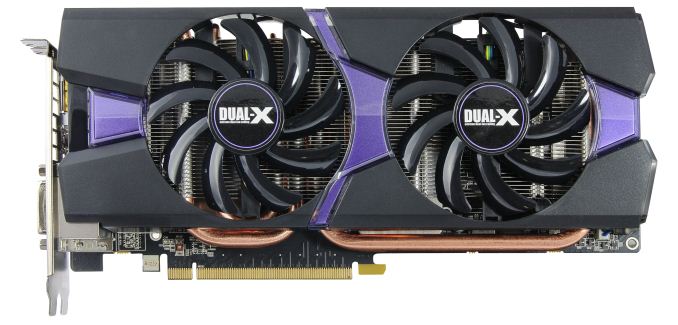
Sapphire's Radeon R9 285 Dual-X
Working for the moment off of the assumption that R9 285 is Tonga based and that it’s a GCN 1.1 part, we expect that performance should be a wash with the R9 280 while the R9 285 has an advantage on features. GCN 1.1 does have some mild performance optimizations to it that will give the R9 285 an edge, though it remains to be seen what the impact will be of the narrower memory bus. The fact that the Tahiti based R9 280X remains in AMD’s lineup indicates that if nothing else, it won’t match the performance of a full Tahiti configuration. Otherwise when it comes to features, being GCN 1.1 based means that the R9 285 will bring with it support for True Audio, support for bridgeless CrossFire thanks to the XDMA engine, GCN 1.1’s superior boost mechanism, and full support for AMD’s upcoming FreeSync implementation of DisplayPort Adaptive Sync (GCN 1.0 GPUs are not fully adaptive).
As for AMD, this offers the chance to refresh some of their oldest GCN 1.0 products with a more capable GPU while also cutting costs. While we don’t have die size numbers for Tonga, it is reasonable to expect that it is smaller due to the narrower memory bus along with the die size optimizations that we saw go into Hawaii last year, which means it will be cheaper to manufacture than Tahiti. This also brings down board costs, again due to the narrower memory bus and the lower TDP allows for simpler power delivery circuitry.
AMD will be positioning the R9 285 to compete with NVIDIA’s GeForce GTX 760, the company’s second-tier GK104 part. The GTX 760 performs roughly the same as the R9 280, so AMD need only not regress to maintain their competitiveness, though any performance lead they can squeeze out will be all for the better. The GTX 760 is frequently found at $239 – a hair under the R9 285’s launch price – so NVIDIA will hold a very slight edge on price assuming they don’t adjust prices further (the GTX 760 launched at $249 almost 14 months ago).
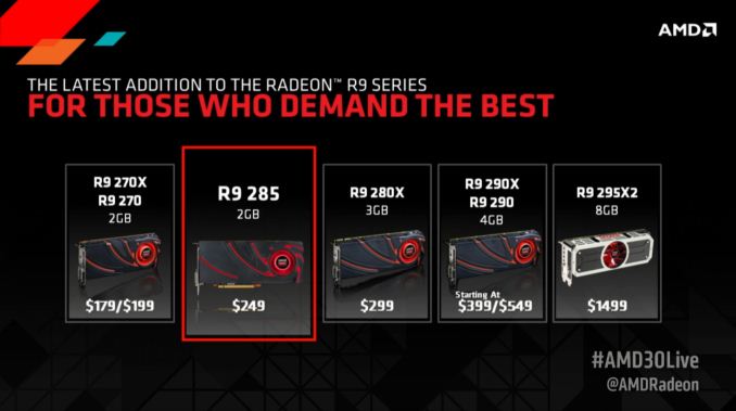
The R9 285 for its part will be launching at $249 on September 2nd. This will be a hard launch, and with AMD’s partners already posting product pages for their designs we suspect this will be a pure virtual (no reference card) launch. AMD also tells us that there will be both 2GB and 4GB cards; we’re going to have to see what the price premium is, as the suitability of 2GB enthusiast cards has been challenged by the presence of so much RAM on the current-generation consoles, which will have a knock-on effect on console-to-PC ports.
Though with the launch of the R9 285 and impending discontinuation of the R9 280, buyers looking at picking up an R9 285 in the near term will have to be on the looking for R9 280 on clearance sale. It’s already regularly found for $220 and lower, making it $30 cheaper than the R9 285 and possessing 3GB of VRAM to the R9 285’s 2GB. This will make the R9 280 a strong contender, at least until supplies run out.
| Fall 2014 GPU Pricing Comparison | |||||
| AMD | Price | NVIDIA | |||
| Radeon R9 290 | $400 | ||||
| $310 | GeForce GTX 770 | ||||
| Radeon R9 280X | $280 | ||||
| Radeon R9 285 | $250 | ||||
| $240 | GeForce GTX 760 | ||||
| Radeon R9 280 | $220 | ||||
| Radeon R9 270X | $180 | ||||
| $160 | GeForce GTX 660 | ||||
Finally, coinciding with the launch of the R9 285 will be a refresh of AMD’s Never Settle bundles. The details on this are still murky at this time, but AMD is launching what they call the Never Settle Space Edition bundle, which will see Alien Isolation and Star Citizen as part of a bundle for all R9 series cards. The lack of clarity is whether this replaces the existing Never Settle Forever bundle in this case, or if these games are being added to the Never Settle Forever lineup in some fashion. AMD has said that current Silver and Gold voucher holders will be able to get the Space Edition bundle with their vouchers, which lends credit to the idea that these are new games in the NSF program rather than a different program entirely.
Both Alien Isolation and Star Citizen are still-in-development games. Alien Isolation is a first person shooter and is expected in October of this year. Meanwhile the space sim Star Citizen does not yet have a release date, and as best as we can tell won’t actually be finished until late 2015 at the earliest. In which case the inclusion here is more about access to the ongoing beta, which is the first time we’ve seen beta access used as part of a bundle in this fashion.





84 Comments
View All Comments
Stuka87 - Saturday, August 23, 2014 - link
I am not sure I understand this card. It looks like it is going to be slower than a 280, but it cost more? Seems like dropping it down to a 256bit bus would be so that they can drop the cost of it, not raise it?Plus the naming scheme is a bit confusing, since the 280X is faster than the 285, but the number is lower.
Rockmandash12 - Saturday, August 23, 2014 - link
It uses the new Tonga chip so it has a lower TDP and it has all the new features like true audio.Frenetic Pony - Saturday, August 23, 2014 - link
Which is cool and all, but doesn't help with the confusing naming part.Mr Perfect - Saturday, August 23, 2014 - link
What someone on another site claimed was that the third digit in the number indicates if it's a refresh part, but the X suffix tells you which is the performance part. Meaning that the 280 refreshes to 285 and 280X refreshes to 285X, but the 280X would still be faster then the 285 since it, well, has an X.If true, it's the most confusing naming convention since... well, they're all pretty bad. But still, bigger number traditionally means faster. This is going to confuse people.
Samus - Sunday, August 24, 2014 - link
I still find it ironic the NVidia GT430 is faster than a GT630 (they're both the same chip but many GT430's had 3200MHz DDR3 on a 128-bit bus.) The confusion is further compounded when you discover there are many GT430's that have a 64-bit bus!It's almost like somebody from GM worked at NVidia and used different revisions without changing the part number...too soon?
Samus - Sunday, August 24, 2014 - link
Dropping the memory bus to 256-bit will have a negligible impact on performance. GCN has an efficient memory controller and 384-bit was always overkill for a 1792 SP configuration. My guess is increasing the bandwidth provided by the 5.5GHz memory is going to offset whatever loss there is from the previous 384-bit memory bus.Although this is an apples to oranges comparison, this is similar to nVidia's strategy where the 770 has a 256-bit bus (~1500 cores) when the 780 has a 384-bit bus (~2300 cores.) NVidia probably found it necessary to implement a 384-bit bus in the same way AMD decided NOT to implement it with the R9 285; they can't saturate a 384-bit bus with "just" 1792 SP's. The transistors saved by reduction of memory bus size can be better utilized elsewhere (or eliminated, reducing power consumption.)
But what's really interesting are the clock speeds. AMD shouldn't have any trouble increasing the clock to 1000MHz and boost to 1100MHz, similar to the 256-bit 270X...how is an essentially simplified Tahiti chip only boosting at 918MHz? You'd assume by now this process would have matured enough to do what nVidia's been successful doing and really push the clock.
ET - Sunday, August 24, 2014 - link
I assume that the low clock is used to lower TDP.TechFanatic - Sunday, August 24, 2014 - link
The low boost clock is likely the direct consequence of Globalfoundries SHP 28nm node.If you recall, a few months back AMD announced that it would be making "specific" GPUs at Globalfoundries and I have it on good authority that Tonga is one of said GPUs.
Globalfoundries 28nm SHP process is more power efficient than TSMCs HP 28nm node but clocks significantly lower.
Which is why we only see a 730mhz boost clock for the integrated GPU in Kaveri.
lefty2 - Sunday, August 24, 2014 - link
The article says that it's TSMC 28nm, not Globalfoundries.Samus - Sunday, August 24, 2014 - link
There is a question mark (?) for manufacturing process in the chart. TSMC's 28nm is, as I said, pretty mature at this point. I don't understand why the clock speed is dropping when millions of transistors are being eliminated by the memory bus reduction, and presumably additional efficiency and tweaks are being added by the revision of Tahiti.This leaves the impression this chip will indeed be a GF part, and that is unfortunate because with high-performance Maxwell parts on the horizon AMD is going to need a miracle to compete over the next 12 months. As far as I'm concerned the 750Ti is the best $150-class GPU you can buy, and it can often be had for $120-$130, effectively undercutting AMD by $50.